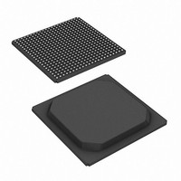
CYD18S72V18-167BGC Cypress Semiconductor Corp, CYD18S72V18-167BGC Datasheet - Page 11

CYD18S72V18-167BGC
Manufacturer Part Number
CYD18S72V18-167BGC
Description
CYD18S72V18-167BGC
Manufacturer
Cypress Semiconductor Corp
Datasheet
1.CYD02S36V18-167BBC.pdf
(52 pages)
Specifications of CYD18S72V18-167BGC
Format - Memory
RAM
Memory Type
SRAM - Dual Port, Synchronous
Memory Size
18M (256K x 72)
Speed
167MHz
Interface
Parallel
Voltage - Supply
1.42 V ~ 1.58 V, 1.7 V ~ 1.9 V
Operating Temperature
0°C ~ 70°C
Package / Case
484-BGA
Lead Free Status / RoHS Status
Contains lead / RoHS non-compliant
Available stocks
Company
Part Number
Manufacturer
Quantity
Price
Company:
Part Number:
CYD18S72V18-167BGC
Manufacturer:
Cypress Semiconductor Corp
Quantity:
10 000
Selectable IO Standard
The FullFlex device families offer the option to choose one of the
four port standards for the device. Each port independently
selects standards from single ended HSTL class I, single ended
LVTTL, 2.5 V LVCMOS, or 1.8 V LVCMOS. The selection of the
standard is determined by the PORTSTD pins for each port.
These pins must be connected to an LVTTL power suppy. This
determines the input clock, address, control, data, and Echo
clock standard for each port as shown in
Table 1. Port Standard Selection
Clocking
Separate clocks synchronize the operations on each port. Each
port has one clock input C. In this mode, all the transactions on
the address, control, and data are on the C rising edge. All
transactions on the address, control, data input, output, and byte
enables occur on the C rising edge.
Table 2. Data Pin Assignment
Selectable Pipelined or Flow through Mode
To meet data rate and throughput requirements, the FullFlex
families offer selectable pipelined or flow through mode. Echo
clocks are not supported in flow through mode and the DLL must
be disabled.
Flow through mode is selected by the FTSEL pin. Strapping this
pin HIGH selects pipelined mode. Strapping this pin LOW selects
flow through mode.
DLL
The FullFlex familes of devices have an on-chip DLL. Enabling
the DLL reduces the clock to data valid (t
setup time for the receiving device. In flow through mode, the
DLL must be disabled. This is selectable by strapping LowSPD
low.
The value in the busy address register is read back to the address lines. The required input control signals for this function are shown
in
as a data read operation. After an initial address match, the BUSY flag is asserted and the address under contention is saved in the
busy address register. All the following address matches enable to generate the BUSY flag. However, none of the addresses are
Document Number: 38-06082 Rev. *J
Table 7
PORTSTD1
VTTL
VTTL
VSS
VSS
BE Pin Name
on page 14. The value in the busy address register is read out to the address lines t
BE[7]
BE[6]
BE[5]
BE[4]
BE[3]
BE[2]
BE[1]
BE[0]
PORTSTD0
VTTL
VTTL
VSS
VSS
Data Pin Name
CD
Table
DQ[71:63]
DQ[62:54]
DQ[53:45]
DQ[44:36]
DQ[35:27]
DQ[26:18]
DQ[17:9]
) time enabling more
DQ[8:0]
2.5 V LVCMOS
1.8 V LVCMOS
I/O Standard
1.
LVTTL
HSTL
Whenever the operating frequency is altered beyond the Clock
Input Cycle to Cycle Jitter specification, reset the DLL, followed
by 1024 clocks before any valid operation.
LowSPD pins are used to reset the DLLs for a single port
independent of all other circuitry. MRST is used to reset all DLLs
on the chip. For more information on DLL lock and reset time,
see
Echo Clocking
As the speed of data increases, on-board delays caused by
parasitics make it extremely difficult to provide accurate clock
trees. To counter this problem, the FullFlex families incorporate
Echo Clocks. Echo Clocks are enabled on a per port basis. The
dual port receives input clocks that are used to clock in the
address and control signals for a read operation. The dual port
retransmits the input clocks relative to the data output. The
buffered clocks are provided on the CQ1/CQ1 and CQ0/CQ0
outputs. Each port has a pair of Echo clocks. Each clock is
associated with half the data bits. The output clock matches the
corresponding ports IO configuration.
To enable echo clock outputs, tie CQEN HIGH. To disable echo
clock outputs, tie CQEN LOW.
Figure 6. SDR Echo Clock Delay
Deterministic Access Control
Deterministic Access Control is provided for ease of design. The
circuitry detects when both ports access the same location and
provides an external BUSY flag to the port on which data is
corrupted. The collision detection logic saves the address in
conflict (Busy Address) to a readable register. In the case of
multiple collisions, the first busy address is written to the busy
address register.
If both ports access the same location at the same time and only
one port is doing a write, if t
and read from the address is valid data. For example, if the right
port is reading and the left port is writing and the left ports clock
meets t
is the old data. In the same case, if the right ports clock meets
t
the new data. In the above case, if t
ports clock with respect to the other port and the right port gets
the external BUSY flag, the data from the right port is corrupted.
Table 3
guarantee the data.
Table 4
and the right port reading, when an external BUSY flag is
asserted on the right port, the data read out of the device is not
guaranteed.
CCS
Data Out
Input Clock
Master Reset on page
, then the data read out of the address from the right port is
Echo Clock
Echo Clock
CCS
on page 12 shows that, in the case of the left port writing
on page 12 shows the t
, then the data read from the address by the right port
18.
CA
CCS
after the same amount of latency
CCS
is met, then the data written to
CCS
timing that must be met to
is violated by the either
Page 11 of 52
FullFlex
[+] Feedback


