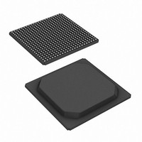
CYD18S72V18-167BGC Cypress Semiconductor Corp, CYD18S72V18-167BGC Datasheet - Page 37

CYD18S72V18-167BGC
Manufacturer Part Number
CYD18S72V18-167BGC
Description
CYD18S72V18-167BGC
Manufacturer
Cypress Semiconductor Corp
Datasheet
1.CYD02S36V18-167BBC.pdf
(52 pages)
Specifications of CYD18S72V18-167BGC
Format - Memory
RAM
Memory Type
SRAM - Dual Port, Synchronous
Memory Size
18M (256K x 72)
Speed
167MHz
Interface
Parallel
Voltage - Supply
1.42 V ~ 1.58 V, 1.7 V ~ 1.9 V
Operating Temperature
0°C ~ 70°C
Package / Case
484-BGA
Lead Free Status / RoHS Status
Contains lead / RoHS non-compliant
Available stocks
Company
Part Number
Manufacturer
Quantity
Price
Company:
Part Number:
CYD18S72V18-167BGC
Manufacturer:
Cypress Semiconductor Corp
Quantity:
10 000
Switching Waveforms
Notes
Document Number: 38-06082 Rev. *J
59. When OE = V
60. Two dummy writes are issued to accomplish bus turnaround. The third instruction is the first valid write.
61. Chip enable or all byte enables are held inactive during the two dummy writes to avoid data corruption.
62. OE is deasserted and t
63. Any write scheduled to complete after OE is deasserted is pre-empted.
R/W
DQ
R/W
OE
C
DQ
A
C
A
DQ
DQ
t
CKLZ2
A
IL
A
x-2
, the last read operation is enabled to complete before the DQ bus is tri-stated and the user is enabled to drive write data.
x
x-2
x
t
CD2
t
CH
t
CYC
t
OHZ
CYC
enabled to elapse before the first write operation is issued.
DQ
t
DQ
t
CL
t
SAC
SAC
Figure 27. READ-to-WRITE for Pipelined Mode (OE Controlled)
A
x-1
Figure 26. READ-to-WRITE for Pipelined Mode (OE = V
x-1
x+1
(continued)
t
t
t
HAC
HAC
DC
DQ
A
x
DQ
n
A
x
t
x+2
OHZ
t
CKHZ2
t
SD
DQ
DQ
A
n
n
n
t
HD
DQ
DQ
A
A
n+1
n+1
n+1
n+1
IL
)
[59, 60, 61]
t
SAC
DQ
t
[62, 63]
SD
DQ
A
A
n+2
n+2
n+2
n+2
t
t
HAC
HD
DQ
A
n+3
n+3
Page 37 of 52
FullFlex
[+] Feedback


