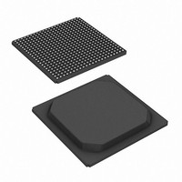
CYD18S72V18-167BGC Cypress Semiconductor Corp, CYD18S72V18-167BGC Datasheet - Page 9

CYD18S72V18-167BGC
Manufacturer Part Number
CYD18S72V18-167BGC
Description
CYD18S72V18-167BGC
Manufacturer
Cypress Semiconductor Corp
Datasheet
1.CYD02S36V18-167BBC.pdf
(52 pages)
Specifications of CYD18S72V18-167BGC
Format - Memory
RAM
Memory Type
SRAM - Dual Port, Synchronous
Memory Size
18M (256K x 72)
Speed
167MHz
Interface
Parallel
Voltage - Supply
1.42 V ~ 1.58 V, 1.7 V ~ 1.9 V
Operating Temperature
0°C ~ 70°C
Package / Case
484-BGA
Lead Free Status / RoHS Status
Contains lead / RoHS non-compliant
Available stocks
Company
Part Number
Manufacturer
Quantity
Price
Company:
Part Number:
CYD18S72V18-167BGC
Manufacturer:
Cypress Semiconductor Corp
Quantity:
10 000
Selection Guide
Pin Definitions
Notes
Document Number: 38-06082 Rev. *J
A[20:0]
DQ[71:0]
BE[7:0]
BUSY
C
CE0
CE1
CQEN
CQ0
CQ0
CQ1
CQ1
ZQ[1:0]
OE
INT
LowSPD
f
Maximum access time (clock to data)
Typical operating current I
Typical standby current for I
20. For 18 Mbit x72 commercial configuration only, refer to
21. SDR mode with two pipelined stages.
22. The CYD36S18V18 device has 21 address bits. The CYD36S36V18 and CYD18S18V18 devices have 20 address bits. The CYD36S72V18, CYD18S36V18, and
23. The FullFlex72 family of devices has 72 data lines. The FullFlex36 family of devices has 36 data lines. The FullFlex18 family of devices has 18 data lines.
24. The FullFlex72 family of devices has eight byte enables. The FullFlex36 family of devices has four byte enables. The FullFlex18 family of devices has two byte enables
25. The pin ZQ[1] is applicable only for 36 Mbit devices. This pin is DNU for 18 Mbit and lower density devices.
MAX
L
L
CYD09S18V18 devices have 19 address bits. The CYD18S72V18, CYD09S36V18, and CYD04S18V18 devices have 18 address bits. The CYD09S72V18 and
CYD04S36V18 devices have 17 address bits. The CYD04S72V18 and CYD02S36V18 have 16 address bits.
L
Left Port
L
L
L
L
L
L
[21]
L
L
L
L
L
L
L
A[20:0]
DQ[71:0]
BE[7:0]
BUSY
C
CE0
CE1
CQEN
CQ0
CQ0
CQ1
CQ1
ZQ[1:0]
OE
INT
LowSPD
R
Right Port
R
R
R
R
R
R
R
R
R
R
R
R
R
CC
R
R
SB3
(both ports CMOS level)
Parameter
Address inputs.
Data bus input and output.
Byte select inputs.
corresponding bytes of the memory array.
Port busy output. When there is an address match and both chip enables are active for both
ports, an external BUSY signal is asserted on the fifth clock cycles from when the collision occurs.
Clock signal. Maximum clock input rate is f
Active LOW chip enable input.
Active HIGH chip enable input.
Echo clock enable input. Assert HIGH to enable echo clocking on respective port.
Echo clock signal output for DQ[35:0] for FullFlex72 devices. Echo clock signal output for
DQ[17:0] for FullFlex36 devices. Echo clock signal output for DQ[8:0] for FullFlex18 devices.
Inverted echo clock signal output for DQ[35:0] for FullFlex72 devices. Inverted echo clock
signal output for DQ[17:0] for FullFlex36 devices. Inverted echo clock signal output for DQ[8:0]
for FullFlex18 devices.
Echo clock signal output for DQ[71:36] for FullFlex72 devices. Echo clock signal output for
DQ[35:18] for FullFlex36 devices. Echo clock signal output for DQ[17:9] for FullFlex18 devices.
Inverted echo clock signal output for DQ[71:36] for FullFlex72 devices. Inverted echo clock
signal output for DQ[35:18] for FullFlex36 devices. Inverted echo clock signal output for DQ[17:9]
for FullFlex18 devices.
VIM output impedance matching input.
and ground. The resistor must be five times larger than the intended line impedance driven by
the dual port. Assert HIGH or leave DNU to disable VIM.
Output enable input. This asynchronous signal must be asserted LOW to enable the DQ data
pins during read operations.
Mailbox interrupt flag output. The mailbox permits communications between ports. The upper
two memory locations are used for message passing. INT
writes to the mailbox location of the left port, and vice versa. An interrupt to a port is deasserted
HIGH when it reads the contents of its mailbox.
Port low speed select input. Assert this pin LOW to disable the DLL. In flow through mode,
this pin needs to be asserted low.
Electrical Characteristics on page 19
[22]
[24]
Asserting these signals enables read and write operations to the
[23]
for complete information.
Description
[25]
MAX
To use, connect a calibrating resistor between ZQ
800
210
.
–200
200
3.3
[20]
[20]
L
is asserted LOW when the right port
700
210
–167
167
4.0
[20]
[20]
FullFlex
Page 9 of 52
MHz
Unit
mA
mA
ns
[+] Feedback


