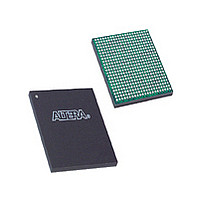
EP3C16F484I7N Altera, EP3C16F484I7N Datasheet - Page 119

EP3C16F484I7N
Manufacturer Part Number
EP3C16F484I7N
Description
Cyclone III
Manufacturer
Altera
Datasheet
1.EP3C16F484I7N.pdf
(274 pages)
Specifications of EP3C16F484I7N
Family Name
Cyclone III
Number Of Logic Blocks/elements
15408
# I/os (max)
346
Frequency (max)
437.5MHz
Process Technology
65nm
Operating Supply Voltage (typ)
1.2V
Logic Cells
15408
Ram Bits
516096
Operating Supply Voltage (min)
1.15V
Operating Supply Voltage (max)
1.25V
Operating Temp Range
-40C to 100C
Operating Temperature Classification
Industrial
Mounting
Surface Mount
Pin Count
484
Package Type
FBGA
Lead Free Status / Rohs Status
Compliant
Available stocks
Company
Part Number
Manufacturer
Quantity
Price
Company:
Part Number:
EP3C16F484I7N
Manufacturer:
ALTERA
Quantity:
4 000
Company:
Part Number:
EP3C16F484I7N
Manufacturer:
ALTERA41
Quantity:
60
Part Number:
EP3C16F484I7N
Manufacturer:
ALTERA/阿尔特拉
Quantity:
20 000
- Current page: 119 of 274
- Download datasheet (6Mb)
Chapter 6: I/O Features in the Cyclone III Device Family
I/O Banks
Table 6–6. Number of VREF Pins Per I/O Banks for Cyclone III and Cyclone III LS Devices (Part 2 of 2)
© December 2009
Family
1
1
Altera Corporation
EP3CLS100
EP3CLS150
EP3CLS200
EP3CLS70
Device
Each I/O bank of the Cyclone III device family has its own VCCIO pins. Each I/O
bank can support only one V
number of supported single-ended or differential standards can be simultaneously
supported in a single I/O bank, as long as they use the same V
output pins.
When designing LVTTL/LVCMOS inputs with Cyclone III and Cyclone III LS
devices, refer to the following guidelines:
■
■
■
Voltage-referenced standards are supported in an I/O bank using any number of
single-ended or differential standards, as long as they use the same V
values. For example, if you choose to implement both SSTL-2 and SSTL-18 in your
Cyclone III and Cyclone III LS devices, I/O pins using these standards—because they
require different V
the same I/O bank can support SSTL-2 and 2.5-V LVCMOS with the V
and the V
When using Cyclone III and Cyclone III LS devices as a receiver in 3.3-, 3.0-, or 2.5-V
LVTTL/LVCMOS systems, you are responsible for managing overshoot or
undershoot to stay in the absolute maximum ratings and the recommended operating
conditions, provided in the
Sheet
The PCI clamping diode is enabled by default in the Quartus II software for input
signals with bank V
All pins accept input voltage (V
recommended operating conditions are provided in the
Sheet
Whenever the input level is higher than the bank V
current.
The LVTTL/LVCMOS I/O standard input pins can only meet the V
levels according to bank voltage level.
chapters.
and
REF
Package
UBGA
UBGA
FBGA
FBGA
FBGA
FBGA
FBGA
FBGA
FBGA
FBGA
set to 1.25 V.
Cyclone III LS Device Data Sheet
REF
CCIO
values—must be in different banks from each other. However,
Pin Count
at 2.5, 3.0, or 3.3 V.
278
278
413
278
278
413
210
413
210
413
Cyclone III Device Data Sheet
CCIO
setting from among 1.2, 1.5, 1.8, 3.0, or 3.3 V. Any
I
1
3
3
3
3
3
3
3
3
3
3
) up to a maximum limit (3.6 V), as stated in the
2
3
3
3
3
3
3
3
3
3
3
chapters.
3
3
3
3
3
3
3
3
3
3
3
CCIO
I/O Banks
4
3
3
3
3
3
3
3
3
3
3
and
Cyclone III Device Handbook, Volume 1
, expect higher leakage
Cyclone III Device Data
Cyclone III LS Device Data
5
3
3
3
3
3
3
3
3
3
3
CCIO
levels for input and
6
3
3
3
3
3
3
3
3
3
3
REF
CCIO
IH
and V
and V
set to 2.5 V
7
3
3
3
3
3
3
3
3
3
3
CCIO
IL
8
3
3
3
3
3
3
3
3
3
3
6–19
Related parts for EP3C16F484I7N
Image
Part Number
Description
Manufacturer
Datasheet
Request
R

Part Number:
Description:
CYCLONE II STARTER KIT EP2C20N
Manufacturer:
Altera
Datasheet:

Part Number:
Description:
CPLD, EP610 Family, ECMOS Process, 300 Gates, 16 Macro Cells, 16 Reg., 16 User I/Os, 5V Supply, 35 Speed Grade, 24DIP
Manufacturer:
Altera Corporation
Datasheet:

Part Number:
Description:
CPLD, EP610 Family, ECMOS Process, 300 Gates, 16 Macro Cells, 16 Reg., 16 User I/Os, 5V Supply, 15 Speed Grade, 24DIP
Manufacturer:
Altera Corporation
Datasheet:

Part Number:
Description:
Manufacturer:
Altera Corporation
Datasheet:

Part Number:
Description:
CPLD, EP610 Family, ECMOS Process, 300 Gates, 16 Macro Cells, 16 Reg., 16 User I/Os, 5V Supply, 30 Speed Grade, 24DIP
Manufacturer:
Altera Corporation
Datasheet:

Part Number:
Description:
High-performance, low-power erasable programmable logic devices with 8 macrocells, 10ns
Manufacturer:
Altera Corporation
Datasheet:

Part Number:
Description:
High-performance, low-power erasable programmable logic devices with 8 macrocells, 7ns
Manufacturer:
Altera Corporation
Datasheet:

Part Number:
Description:
Classic EPLD
Manufacturer:
Altera Corporation
Datasheet:

Part Number:
Description:
High-performance, low-power erasable programmable logic devices with 8 macrocells, 10ns
Manufacturer:
Altera Corporation
Datasheet:

Part Number:
Description:
Manufacturer:
Altera Corporation
Datasheet:

Part Number:
Description:
Manufacturer:
Altera Corporation
Datasheet:

Part Number:
Description:
Manufacturer:
Altera Corporation
Datasheet:

Part Number:
Description:
CPLD, EP610 Family, ECMOS Process, 300 Gates, 16 Macro Cells, 16 Reg., 16 User I/Os, 5V Supply, 25 Speed Grade, 24DIP
Manufacturer:
Altera Corporation
Datasheet:


