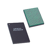
EP3C16F484I7N Altera, EP3C16F484I7N Datasheet - Page 47

EP3C16F484I7N
Manufacturer Part Number
EP3C16F484I7N
Description
Cyclone III
Manufacturer
Altera
Datasheet
1.EP3C16F484I7N.pdf
(274 pages)
Specifications of EP3C16F484I7N
Family Name
Cyclone III
Number Of Logic Blocks/elements
15408
# I/os (max)
346
Frequency (max)
437.5MHz
Process Technology
65nm
Operating Supply Voltage (typ)
1.2V
Logic Cells
15408
Ram Bits
516096
Operating Supply Voltage (min)
1.15V
Operating Supply Voltage (max)
1.25V
Operating Temp Range
-40C to 100C
Operating Temperature Classification
Industrial
Mounting
Surface Mount
Pin Count
484
Package Type
FBGA
Lead Free Status / Rohs Status
Compliant
Available stocks
Company
Part Number
Manufacturer
Quantity
Price
Company:
Part Number:
EP3C16F484I7N
Manufacturer:
ALTERA
Quantity:
4 000
Company:
Part Number:
EP3C16F484I7N
Manufacturer:
ALTERA41
Quantity:
60
Part Number:
EP3C16F484I7N
Manufacturer:
ALTERA/阿尔特拉
Quantity:
20 000
- Current page: 47 of 274
- Download datasheet (6Mb)
Chapter 3: Memory Blocks in the Cyclone III Device Family
Memory Modes
Figure 3–10. Cyclone III Device Family Simple Dual-Port Timing Waveforms
True Dual-Port Mode
© December 2009
q (asynch)
wraddress
rdaddress
wrclock
rdclock
wren
data
rden
1
Altera Corporation
din-1
doutn-1
an-1
Figure 3–10
dual-port mode with unregistered outputs. Registering the outputs of the RAM
simply delays the q output by one clock cycle.
True dual-port mode supports any combination of two-port operations: two reads,
two writes, or one read and one write, at two different clock frequencies.
shows the Cyclone III device family true dual-port memory configuration.
Figure 3–11. Cyclone III Device Family True Dual-Port Memory
Note to
(1) True dual-port memory supports input or output clock mode in addition to the independent clock mode shown.
The widest bit configuration of the M9K blocks in true dual-port mode is 512 × 16-bit
(18-bit with parity).
bn
Figure
an
din
3–11:
shows the timing waveforms for read and write operations in simple
doutn
b0
a0
a1
data_a[ ]
address_a[ ]
wren_a
byteena_a[]
addressstall_a
clocken_a
rden_a
aclr_a
q_a[]
clock_a
dout0
a2
b1
a3
addressstall_b
address_b[]
byteena_b[]
clocken_b
data_b[ ]
clock_b
wren_b
rden_b
aclr_b
q_b[]
din4
b2
a4
(Note 1)
Cyclone III Device Handbook, Volume 1
din5
a5
b3
a6
din6
Figure 3–11
3–11
Related parts for EP3C16F484I7N
Image
Part Number
Description
Manufacturer
Datasheet
Request
R

Part Number:
Description:
CYCLONE II STARTER KIT EP2C20N
Manufacturer:
Altera
Datasheet:

Part Number:
Description:
CPLD, EP610 Family, ECMOS Process, 300 Gates, 16 Macro Cells, 16 Reg., 16 User I/Os, 5V Supply, 35 Speed Grade, 24DIP
Manufacturer:
Altera Corporation
Datasheet:

Part Number:
Description:
CPLD, EP610 Family, ECMOS Process, 300 Gates, 16 Macro Cells, 16 Reg., 16 User I/Os, 5V Supply, 15 Speed Grade, 24DIP
Manufacturer:
Altera Corporation
Datasheet:

Part Number:
Description:
Manufacturer:
Altera Corporation
Datasheet:

Part Number:
Description:
CPLD, EP610 Family, ECMOS Process, 300 Gates, 16 Macro Cells, 16 Reg., 16 User I/Os, 5V Supply, 30 Speed Grade, 24DIP
Manufacturer:
Altera Corporation
Datasheet:

Part Number:
Description:
High-performance, low-power erasable programmable logic devices with 8 macrocells, 10ns
Manufacturer:
Altera Corporation
Datasheet:

Part Number:
Description:
High-performance, low-power erasable programmable logic devices with 8 macrocells, 7ns
Manufacturer:
Altera Corporation
Datasheet:

Part Number:
Description:
Classic EPLD
Manufacturer:
Altera Corporation
Datasheet:

Part Number:
Description:
High-performance, low-power erasable programmable logic devices with 8 macrocells, 10ns
Manufacturer:
Altera Corporation
Datasheet:

Part Number:
Description:
Manufacturer:
Altera Corporation
Datasheet:

Part Number:
Description:
Manufacturer:
Altera Corporation
Datasheet:

Part Number:
Description:
Manufacturer:
Altera Corporation
Datasheet:

Part Number:
Description:
CPLD, EP610 Family, ECMOS Process, 300 Gates, 16 Macro Cells, 16 Reg., 16 User I/Os, 5V Supply, 25 Speed Grade, 24DIP
Manufacturer:
Altera Corporation
Datasheet:


