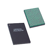
EP3C16F484I7N Altera, EP3C16F484I7N Datasheet - Page 231

EP3C16F484I7N
Manufacturer Part Number
EP3C16F484I7N
Description
Cyclone III
Manufacturer
Altera
Datasheet
1.EP3C16F484I7N.pdf
(274 pages)
Specifications of EP3C16F484I7N
Family Name
Cyclone III
Number Of Logic Blocks/elements
15408
# I/os (max)
346
Frequency (max)
437.5MHz
Process Technology
65nm
Operating Supply Voltage (typ)
1.2V
Logic Cells
15408
Ram Bits
516096
Operating Supply Voltage (min)
1.15V
Operating Supply Voltage (max)
1.25V
Operating Temp Range
-40C to 100C
Operating Temperature Classification
Industrial
Mounting
Surface Mount
Pin Count
484
Package Type
FBGA
Lead Free Status / Rohs Status
Compliant
Available stocks
Company
Part Number
Manufacturer
Quantity
Price
Company:
Part Number:
EP3C16F484I7N
Manufacturer:
ALTERA
Quantity:
4 000
Company:
Part Number:
EP3C16F484I7N
Manufacturer:
ALTERA41
Quantity:
60
Part Number:
EP3C16F484I7N
Manufacturer:
ALTERA/阿尔特拉
Quantity:
20 000
- Current page: 231 of 274
- Download datasheet (6Mb)
Chapter 9: Configuration, Design Security, and Remote System Upgrades in the Cyclone III Device Family
Configuration Features
Table 9–22. Dedicated Configuration Pins on Cyclone III Device Family (Part 4 of 4)
© December 2009
DATA[7..2]
DATA[15..8]
PADD[23..0]
nRESET
nAVD
nOE
nWE
Note to
(1) AP configuration scheme is for Cyclone III devices only.
Pin Name
Table
9–22:
Altera Corporation
Mode
User
I/O
I/O
I/O
I/O
I/O
I/O
I/O
Configuration
FPP, AP
Scheme
AP
AP
AP
AP
AP
AP
(1)
(1)
(1)
(1)
(1)
(1)
(1)
Bidirectional
Bidirectional
Pin Type
(AP)
Output
Output
Output
Output
Output
Inputs
(FPP).
(1)
Data inputs.
In AS or PS configuration schemes, they function as user I/O
pins during configuration, which means they are tri-stated.
After FPP configuration, DATA[7..2] are available as user
I/O pins and the state of these pin depends on the
Dual-Purpose Pin settings.
The byte-wide or word-wide configuration data is presented
to the target Cyclone III device on
DATA[15..0] , respectively, in the AP configuration
scheme (for Cyclone III devices only). After AP configuration,
DATA[7..2] are dedicated bidirectional pins with optional
user control.
Data inputs. Word-wide configuration data is presented to the
target Cyclone III device on DATA[15..0].
In PS, FPP, or AS configuration schemes, they function as
user I/O pins during configuration, which means they are
tri-stated.
After AP configuration, DATA[15:8] are dedicated
bidirectional pins with optional user control.
24-bit address bus from the Cyclone III device to the parallel
flash in AP mode. Connects to the A[24:1] bus on the
Numonyx P30 or P33 flash.
Active-low reset output. Driving the nRESET pin low resets
the parallel flash. Connects to the RST# pin on the Numonyx
P30 or P33 flash.
Active-low address valid output. Driving the nAVD pin low
during a read or write operation indicates to the parallel flash
that valid address is present on the PADD[23..0] address
bus. Connects to the ADV# pin on the Numonyx P30 or P33
flash.
Active-low output enable to the parallel flash. Driving the
nOE pin low during a read operation enables the parallel flash
outputs (DATA[15..0]). Connects to the OE# pin on the
Numonyx P30 or P33 flash.
Active-low write enable to the parallel flash. Driving the nWE
pin low during a write operation indicates to the parallel flash
that data on the DATA[15..0] bus is valid. Connects to
the WE# pin on the Numonyx P30 or P33 flash.
(1)
Description
Cyclone III Device Handbook, Volume 1
DATA[7..0] or
9–71
Related parts for EP3C16F484I7N
Image
Part Number
Description
Manufacturer
Datasheet
Request
R

Part Number:
Description:
CYCLONE II STARTER KIT EP2C20N
Manufacturer:
Altera
Datasheet:

Part Number:
Description:
CPLD, EP610 Family, ECMOS Process, 300 Gates, 16 Macro Cells, 16 Reg., 16 User I/Os, 5V Supply, 35 Speed Grade, 24DIP
Manufacturer:
Altera Corporation
Datasheet:

Part Number:
Description:
CPLD, EP610 Family, ECMOS Process, 300 Gates, 16 Macro Cells, 16 Reg., 16 User I/Os, 5V Supply, 15 Speed Grade, 24DIP
Manufacturer:
Altera Corporation
Datasheet:

Part Number:
Description:
Manufacturer:
Altera Corporation
Datasheet:

Part Number:
Description:
CPLD, EP610 Family, ECMOS Process, 300 Gates, 16 Macro Cells, 16 Reg., 16 User I/Os, 5V Supply, 30 Speed Grade, 24DIP
Manufacturer:
Altera Corporation
Datasheet:

Part Number:
Description:
High-performance, low-power erasable programmable logic devices with 8 macrocells, 10ns
Manufacturer:
Altera Corporation
Datasheet:

Part Number:
Description:
High-performance, low-power erasable programmable logic devices with 8 macrocells, 7ns
Manufacturer:
Altera Corporation
Datasheet:

Part Number:
Description:
Classic EPLD
Manufacturer:
Altera Corporation
Datasheet:

Part Number:
Description:
High-performance, low-power erasable programmable logic devices with 8 macrocells, 10ns
Manufacturer:
Altera Corporation
Datasheet:

Part Number:
Description:
Manufacturer:
Altera Corporation
Datasheet:

Part Number:
Description:
Manufacturer:
Altera Corporation
Datasheet:

Part Number:
Description:
Manufacturer:
Altera Corporation
Datasheet:

Part Number:
Description:
CPLD, EP610 Family, ECMOS Process, 300 Gates, 16 Macro Cells, 16 Reg., 16 User I/Os, 5V Supply, 25 Speed Grade, 24DIP
Manufacturer:
Altera Corporation
Datasheet:


