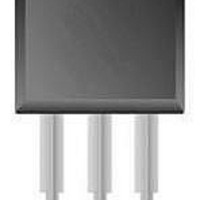
J176 AMO NXP Semiconductors, J176 AMO Datasheet - Page 5

J176 AMO
Manufacturer Part Number
J176 AMO
Description
RF JFET AMMORA FET-RFSS
Manufacturer
NXP Semiconductors
Specifications of J176 AMO
Configuration
Single
Mounting Style
Through Hole
Minimum Operating Temperature
- 65 C
Transistor Polarity
P-Channel
Drain Source Voltage Vds
30 V
Gate-source Breakdown Voltage
30 V
Maximum Drain Gate Voltage
30 V
Continuous Drain Current
35 mA
Maximum Operating Temperature
+ 150 C
Package / Case
SPT
Channel Type
P
Gate-source Voltage (max)
30V
Drain Current (max)
35mA
Drain-gate Voltage (max)
30V
Drain-source Volt (max)
30V
Operating Temperature (max)
150C
Operating Temperature Classification
Military
Mounting
Through Hole
Pin Count
3
Package Type
SOT-23
Lead Free Status / RoHS Status
Lead free / RoHS Compliant
Other names
J176,126
PACKAGE OUTLINE
Plastic single-ended leaded (through hole) package; 3 leads
Philips Semiconductors
April 1995
DIMENSIONS (mm are the original dimensions)
Note
1. Terminal dimensions within this zone are uncontrolled to allow for flow of plastic and terminal irregularities.
P-channel silicon field-effect transistors
UNIT
mm
VERSION
OUTLINE
SOT54
D
5.2
5.0
A
0.48
0.40
d
b
E
3
1
2
0.66
0.56
b 1
IEC
b
1
0.45
0.40
c
4.8
4.4
D
JEDEC
TO-92
1.7
1.4
d
REFERENCES
0
4.2
3.6
E
2.54
A
e
SC-43
scale
EIAJ
2.5
5
1.27
e 1
14.5
12.7
5 mm
L
L 1
L 1
2.5
(1)
L
PROJECTION
EUROPEAN
Product specification
J174; J175;
J176; J177
ISSUE DATE
b
97-02-28
c
e 1
e
SOT54


