STTH3R02 STMicroelectronics, STTH3R02 Datasheet
STTH3R02
Specifications of STTH3R02
Available stocks


Related parts for STTH3R02


STTH3R02 Summary of contents
Page 1
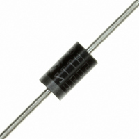
... Low forward and reverse recovery times ■ High junction temperature Description The STTH3R02 uses ST's new 200 V planar Pt doping technology, and it is specially suited for switching mode base drive and transistor circuits. Packaged in DO-201AD, DO-15, and SMC, this device is intended for use in low voltage, high frequency inverters, free wheeling and polarity protection ...
Page 2
... 150° (RMS) Value 200 110 50° C lead = 90° lead = 110° - 175 175 230 Value DO-15 45 DO-201AD 30 SMC 20 Min. Typ = V RRM 3 0.89 0.76 0.70 STTH3R02 Unit ° C ° C ° C Unit ° C/W Max. Unit 3 µA 30 1.20 1.0 V 0.85 0.80 ...
Page 3
... STTH3R02 Table 4. Dynamic characteristics Symbol Parameter t Reverse recovery time rr I Reverse recovery current RM t Forward recovery time fr V Forward recovery voltage FP Figure 1. peak current versus duty cycle 100 δ 0 0.0 0.1 0.2 0.3 0.4 0.5 Figure 3. Forward voltage drop versus forward current (maximum values) ...
Page 4
... CU SMC =1cm² (s) P 1.E-02 1.E-01 1.E+00 1.E+01 1.E+02 Reverse recovery charges versus dI /dt (typical values = =160V R T =125° =25° 100 versus dI /dt (typical values =3A F =160V T =125° =25° 100 STTH3R02 1.E+03 /dt(A/µs) 1000 /dt(A/µs) F 1000 ...
Page 5
... STTH3R02 Figure 11. Dynamic parameters versus junction temperature 1 =160V 1 0.8 0 0.4 0.2 0 Figure 13. Thermal resistance versus copper surface under each lead for SMC (Epoxy printed circuit board FR4 35µm) CU 100 (cm² 0.0 0.5 1.0 1.5 2.0 2.5 2 Ordering information scheme Figure 12 ...
Page 6
... The minimum length which must stay straight between the right angles after bending is 0.59"(15mm) Dimensions Ref. Millimeters Min. Max. Min. A 6.05 6.75 0.238 B 2.95 3.53 0.116 1.024 D 0.71 0.88 0.028 STTH3R02 Inches Max. 0.374 0.209 0.051 0.049 Inches Max. 0.266 0.139 1.220 0.035 ...
Page 7
... STTH3R02 Table 7. SMC dimensions Figure 15. SMC footprint (dimensions in mm) In order to meet environmental requirements, ST offers these devices in ECOPACK® packages. These packages have a lead-free second level interconnect. The category of second level interconnect is marked on the package and on the inner box label, in compliance with JEDEC Standard JESD97. The maximum ratings related to soldering conditions are also marked on the inner box label ...
Page 8
... Ordering information Part Number STTH3R02 STTH3R02RL STTH3R02Q STTH3R02QRL STTH3R02S 5 Revision history Date 03-May-2006 10-Oct-2006 8/9 Marking Package STTH3R02 DO-201AD STTH3R02 DO-201AD STTH3R02 DO-15 STTH3R02 DO-15 3R2S SMC Revision Description of Changes 1 First issue 2 Added SMC package STTH3R02 Weight Base qty Delivery mode 1 ...
Page 9
... STTH3R02 Information in this document is provided solely in connection with ST products. STMicroelectronics NV and its subsidiaries (“ST”) reserve the right to make changes, corrections, modifications or improvements, to this document, and the products and services described herein at any time, without notice. All ST products are sold pursuant to ST’s terms and conditions of sale. ...