STGW40NC60W STMicroelectronics, STGW40NC60W Datasheet
STGW40NC60W
Specifications of STGW40NC60W
Available stocks


Related parts for STGW40NC60W


STGW40NC60W Summary of contents
Page 1
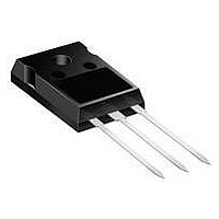
... This IGBT utilizes the advanced PowerMESH™ process resulting in an excellent trade-off between switching performance and low on-state behavior. Table 1. Device summary Order code STGW40NC60W July 2008 600 V - ultra fast IGBT Figure 1. Marking Package GW40NC60W TO-247 Rev 1 STGW40NC60W TO-247 Internal schematic diagram Packaging Tube www.st.com 1/13 13 ...
Page 2
... Contents Contents 1 Electrical ratings . . . . . . . . . . . . . . . . . . . . . . . . . . . . . . . . . . . . . . . . . . . . 3 2 Electrical characteristics . . . . . . . . . . . . . . . . . . . . . . . . . . . . . . . . . . . . . 4 2.1 Electrical characteristics (curves) 3 Test circuit . . . . . . . . . . . . . . . . . . . . . . . . . . . . . . . . . . . . . . . . . . . . . . . . 9 4 Package mechanical data . . . . . . . . . . . . . . . . . . . . . . . . . . . . . . . . . . . . 10 5 Revision history . . . . . . . . . . . . . . . . . . . . . . . . . . . . . . . . . . . . . . . . . . . 12 2/13 STGW40NC60W . . . . . . . . . . . . . . . . . . . . . . . . . . . . 6 ...
Page 3
... STGW40NC60W 1 Electrical ratings Table 2. Absolute maximum ratings Symbol Collector-emitter voltage (V V CES (1) I Collector current (continuous °C C (1) I Collector current (continuous) at 100 °C C (2) I Turn-off latching current CL (3) Pulsed collector current Gate-emitter voltage GE Total dissipation TOT T Operating junction temperature j 1. Calculated according to the iterative formula: ...
Page 4
... Gate-collector charge Q gc 4/13 Parameter Test conditions 600 600 ± Parameter Test conditions MHz 390 (see Figure 17) STGW40NC60W Min. Typ. Max. Unit 600 = =125 °C 1 250µA 3.75 C =125 ° Min. Typ. Max. Unit 2900 = 0 298 126 2 5.75 V 500 µ ±100 ...
Page 5
... STGW40NC60W Table 6. Switching on/off (inductive load) Symbol t Turn-on delay time d(on) t Current rise time r Turn-on current slope (di/dt Turn-on delay time d(on) t Current rise time r Turn-on current slope (di/dt Off voltage rise time r off Turn-off delay time d off Current fall time ...
Page 6
... Electrical characteristics 2.1 Electrical characteristics (curves) Figure 2. Output characteristics Figure 4. Transconductance Figure 6. Collector-emitter on voltage vs collector current 6/13 Figure 3. Transfer characteristics Figure 5. Collector-emitter on voltage vs temperature Figure 7. Normalized gate threshold vs temperature STGW40NC60W ...
Page 7
... STGW40NC60W Figure 8. Normalized breakdown voltage vs temperature Figure 10. Capacitance variations Figure 12. Switching losses vs gate resistance Figure 13. Switching losses vs collector Electrical characteristics Figure 9. Gate charge vs gate-emitter voltage Figure 11. Switching losses vs temperature current 7/13 ...
Page 8
... Electrical characteristics Figure 14. Thermal impedance 8/13 Figure 15. Turn-off SOA STGW40NC60W ...
Page 9
... STGW40NC60W 3 Test circuit Figure 16. Test circuit for inductive load switching Figure 18. Switching waveforms Figure 17. Gate charge test circuit Test circuit 9/13 ...
Page 10
... These packages have a Lead-free second level interconnect. The category of second level interconnect is marked on the package and on the inner box label, in compliance with JEDEC Standard JESD97. The maximum ratings related to soldering conditions are also marked on the inner box label. ECOPACK trademark. ECOPACK specifications are available at: 10/13 www.st.com STGW40NC60W ...
Page 11
... STGW40NC60W Dim øP øR S TO-247 Mechanical data mm. Min. Typ 4.85 2.20 1.0 2.0 3.0 0.40 19.85 15.45 5.45 14.20 3.70 18.50 3.55 4.50 5.50 Package mechanical data Max. 5.15 2.60 1.40 2.40 3.40 0.80 20.15 15.75 14.80 4.30 3.65 5.50 11/13 ...
Page 12
... Revision history 5 Revision history Table 8. Document revision history Date 09-Jul-2008 12/13 Revision 1 First release STGW40NC60W Changes ...
Page 13
... STGW40NC60W Information in this document is provided solely in connection with ST products. STMicroelectronics NV and its subsidiaries (“ST”) reserve the right to make changes, corrections, modifications or improvements, to this document, and the products and services described herein at any time, without notice. All ST products are sold pursuant to ST’s terms and conditions of sale. ...