STGW20NC60VD STMicroelectronics, STGW20NC60VD Datasheet
STGW20NC60VD
Specifications of STGW20NC60VD
Available stocks


Related parts for STGW20NC60VD


STGW20NC60VD Summary of contents
Page 1
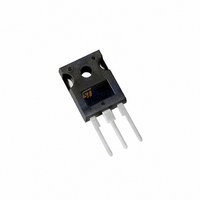
... N-CHANNEL 30A - 600V TO-247 Very Fast PowerMESH™ IGBT Figure 1: Package (Max) I CE(sat) C @25°C @100°C < 2 Figure 2: Internal Schematic Diagram MARKING PACKAGE GW20NC60VD STGW20NC60VD TO-247 Weight: 4.41gr ± 0.01 Max Clip Pressure: 150 N/mm PACKAGING TO-247 TUBE Rev. 4 1/11 ...
Page 2
... STGW20NC60VD Table 3: Absolute Maximum ratings Symbol V Collector-Emitter Voltage (V CES V Reverse Battery Protection ECR V Gate-Emitter Voltage GE I Collector Current (continuous) at 25°C (#) C I Collector Current (continuous) at 100°C (#) C I (1) Collector Current (pulsed Diode RMS Forward Current Total Dissipation at T TOT Derating Factor ...
Page 3
... V = 390 3 15V, Tj 125°C (see Figure 19) Test Conditions V = 390 3 °C J (see Figure 19 390 3 125 °C (see Figure 19) STGW20NC60VD Min. Typ. Max. Unit 15 S 2200 pF 225 100 140 100 A Min. Typ. Max. Unit 1600 A/µs 220 300 µ 11.5 ns 1500 A/µs 450 µ ...
Page 4
... STGW20NC60VD Table 10: Collector-Emitter Diode Symbol Parameter V Forward On-Voltage f t Reverse Recovery Time Reverse Recovery Charge Q rr Reverse Recovery Current I rrm Softness factor of the diode S t Reverse Recovery Time Reverse Recovery Charge Q rr Reverse Recovery Current I rrm Softness factor of the diode S 4/11 ...
Page 5
... Figure 3: Output Characteristics Figure 4: Transconductance Figure 5: Collector-Emitter On Voltage vs Col- lector Current STGW20NC60VD Figure 6: Transfer Characteristics Figure 7: Collector-Emitter On Voltage vs Tem- perature Figure 8: Normalized Gate Threshold vs Tem- perature 5/11 ...
Page 6
... STGW20NC60VD Figure 9: Normalized Breakdown Voltage vs Temperature Figure 10: Capacitance Variations Figure 11: Total Switching Losses vs Gate Re- sistance 6/11 Figure 12: Gate Charge vs Gate-Emitter Volt- age Figure 13: Total Switching Losses vs Temper- ature Figure 14: Total Switching Losses vs Collector Current ...
Page 7
... Figure 15: Thermal Impedance Figure 16: Turn-Off SOA Figure 17: Emitter-Collector Diode Character- istics STGW20NC60VD Figure 18 Frequency For a fast IGBT suitable for high frequency appli- cations, the typical collector current vs. maximum operating frequency curve is reported. That fre- quency is defined as follows MAX The maximum power dissipation is limited by ...
Page 8
... STGW20NC60VD Figure 19: Test Circuit for Inductive Load Switching Figure 20: Switching Waveforms 8/11 Figure 21: Gate Charge Test Circuit Figure 22: Diode Recovery Times Waveform ...
Page 9
... Table 11: Revision History Date Revision 12-July-2004 4 Description of Changes Stylesheet update. Added Max Values see Table 8 and 9 Added Figure 22 STGW20NC60VD 9/11 ...
Page 10
... STGW20NC60VD DIM. MIN. A 4.85 A1 2.20 b 1.0 b1 2.0 b2 3.0 c 0.40 D 19.85 E 15. 14.20 L1 3.70 L2 øP 3.55 øR 4.50 S 10/11 TO-247 MECHANICAL DATA mm. TYP MAX. MIN. 5.15 0.19 2.60 0.086 1.40 0.039 2.40 0.079 3.40 0.118 0.80 0.015 20.15 0.781 15.75 0.608 5.45 14 ...
Page 11
... All other names are the property of their respective owners Australia - Belgium - Brazil - Canada - China - Czech Republic - Finland - France - Germany - Hong Kong - India - Israel - Italy - Japan - Malaysia - Malta - Morocco - Singapore - Spain - Sweden - Switzerland - United Kingdom - United States. © 2004 STMicroelectronics - All Rights Reserved STMicroelectronics GROUP OF COMPANIES STGW20NC60VD 11/11 ...