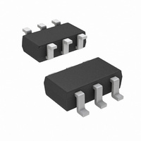
SI3850ADV-T1-E3 Vishay, SI3850ADV-T1-E3 Datasheet

SI3850ADV-T1-E3
Specifications of SI3850ADV-T1-E3
Related parts for SI3850ADV-T1-E3
SI3850ADV-T1-E3 Summary of contents
Page 1
... Ordering Information: Si3850ADV-T1-E3 (Lead (Pb)-free) ABSOLUTE MAXIMUM RATINGS T Parameter Drain-Source Voltage Gate-Source Voltage Continuous Drain Current (T = 150 °C) J Pulsed Drain Current Continuous Source Current (Diode Conduction) Maximum Power Dissipation (Surface Mounted on FR4 Board) Operating Junction and Storage Temperature Range THERMAL RESISTANCE RATINGS ...
Page 2
... Si3850ADV Vishay Siliconix SPECIFICATIONS °C, unless otherwise noted J Parameter Symbol Static V Gate Threshold Voltage Gate-Body Leakage Zero Gate Voltage Drain Current b On-State Drain Current b r Drain-Source On-State Resistance b Forward Transconductance b Diode Forward Voltage b Dynamic Total Gate Charge Gate-Source Charge Gate-Drain Charge ...
Page 3
... Q – Total Gate Charge (nC) g Gate Charge Document Number: 73789 S-60470-Rev. A, 27-Mar- 2 2.1 2 2.0 2.5 3.0 3 1.5 2.0 2.5 Si3850ADV Vishay Siliconix 3 °C 2.4 25 °C 1.8 T 1.2 0.6 0 – Gate-to-Source Voltage (V) GS Transfer Characteristics 110 iss 44 C oss 22 ...
Page 4
... Si3850ADV Vishay Siliconix N-CHANNEL TYPICAL CHARACTERISTICS 25 °C, unless noted 10 150 °C 1 0.1 0.01 0.001 0.0 0.3 0.6 V – Source-to-Drain Voltage (V) SD Source-Drain Diode Forward Voltage 0.2 0.1 - 0.0 - 0.1 - 0.2 - 0 – Temperature (°C) J Threshold Voltage www.vishay.com 4 25 °C 0.9 1.2 1 ...
Page 5
... N-CHANNEL TYPICAL CHARACTERISTICS 25 °C, unless noted 1 Duty Cycle = 0.5 0.2 0.1 0.1 0.05 0.02 Single Pulse 0. Document Number: 73789 S-60470-Rev. A, 27-Mar- Square Wave Pulse Duration (sec) Normalized Thermal Transient Impedance, Junction-to-Ambient Si3850ADV Vishay Siliconix Notes Duty Cycle Per Unit Base = R = 100 °C/W thJA ( – ...
Page 6
... Si3850ADV Vishay Siliconix P-CHANNEL TYPICAL CHARACTERISTICS 25 °C, unless noted 2.5 2.0 1.5 1.0 0.5 0.0 0.0 0.5 1.0 1.5 V – Drain-to-Source Voltage (V) DS Output Characteristics 2 1.5 1.0 0.5 0.0 0.0 0.5 1.0 I – Drain Current (A) D On-Resistance vs. Drain Current ...
Page 7
... DS(on °C A Single Pulse BV Limited DSS 0. – Drain-to-Source Voltage ( minimum V at which DS(on) Safe Operating Area Si3850ADV Vishay Siliconix 3.0 2.4 1.8 125 °C 1.2 25 °C 0.6 0 – Gate-to-Source Voltage (V) GS On-Resistance vs. Gate-to-Source Voltage 0.001 0.01 ...
Page 8
... Si3850ADV Vishay Siliconix P-CHANNEL TYPICAL CHARACTERISTICS 25 °C, unless noted 1 Duty Cycle = 0.5 0.2 0.1 0.1 0.05 0.02 Single Pulse 0. Vishay Siliconix maintains worldwide manufacturing capability. Products may be manufactured at one of several qualified locations. Reliability data for Silicon Tech- nology and Package Reliability represent a composite of all qualified locations. For related documents such as package/tape drawings, part marking, and reliability data, see http://www ...
Page 9
... Vishay disclaims any and all liability arising out of the use or application of any product described herein or of any information provided herein to the maximum extent permitted by law. The product specifications do not expand or otherwise modify Vishay’ ...


