SI3853DV-T1-E3 Vishay, SI3853DV-T1-E3 Datasheet - Page 2
SI3853DV-T1-E3
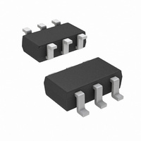
Manufacturer Part Number
SI3853DV-T1-E3
Description
MOSFET P-CH 20V 1.6A 6-TSOP
Manufacturer
Vishay
Datasheet
1.SI3853DV-T1-E3.pdf
(7 pages)
Specifications of SI3853DV-T1-E3
Transistor Polarity
P-Channel
Fet Type
MOSFET P-Channel, Metal Oxide
Fet Feature
Diode (Isolated)
Rds On (max) @ Id, Vgs
200 mOhm @ 1.8A, 4.5V
Drain To Source Voltage (vdss)
20V
Current - Continuous Drain (id) @ 25° C
1.6A
Vgs(th) (max) @ Id
500mV @ 250µA
Gate Charge (qg) @ Vgs
4nC @ 4.5V
Power - Max
830mW
Mounting Type
Surface Mount
Package / Case
6-TSOP
Minimum Operating Temperature
- 55 C
Configuration
Single
Resistance Drain-source Rds (on)
0.2 Ohms
Drain-source Breakdown Voltage
- 20 V
Gate-source Breakdown Voltage
+/- 12 V
Continuous Drain Current
+/- 1.6 A
Power Dissipation
0.83 W
Maximum Operating Temperature
+ 150 C
Mounting Style
SMD/SMT
Continuous Drain Current Id
1.8A
Drain Source Voltage Vds
-20V
On Resistance Rds(on)
200mohm
Rds(on) Test Voltage Vgs
-4.5V
Power Dissipation Pd
830mW
No. Of Pins
6
Lead Free Status / RoHS Status
Lead free / RoHS Compliant
Lead Free Status / RoHS Status
Lead free / RoHS Compliant, Lead free / RoHS Compliant
Other names
SI3853DV-T1-E3TR
Available stocks
Company
Part Number
Manufacturer
Quantity
Price

Part Number:
SI3853DV-T1-E3
Manufacturer:
VISHAY/威世
Quantity:
20 000


Si3853DV
Vishay Siliconix
Notes:
a. Surface mounted on 1" x 1" FR4 board.
Notes:
a. Pulse test; pulse width ≤ 300 µs, duty cycle ≤ 2 %.
b. Guaranteed by design, not subject to production testing.
Stresses beyond those listed under “Absolute Maximum Ratings” may cause permanent damage to the device. These are stress ratings only, and functional operation
of the device at these or any other conditions beyond those indicated in the operational sections of the specifications is not implied. Exposure to absolute maximum
rating conditions for extended periods may affect device reliability.
www.vishay.com
2
THERMAL RESISTANCE RATINGS
Parameter
Junction-to-Ambient
Junction-to-Foot
MOSFET SPECIFICATIONS T
Parameter
Static
Gate Threshold Voltage
Gate-Body Leakage
Zero Gate Voltage Drain Current
On-State Drain Current
Drain-Source On-State Resistance
Forward Transconductance
Diode Forward Voltage
Dynamic
Total Gate Charge
Gate-Source Charge
Gate-Drain Charge
Turn-On Delay Time
Rise Time
Turn-Off DelayTime
Fall Time
Body Diode Reverse Recovery Time
SCHOTTKY SPECIFICATIONS T
Parameter
Forward Voltage Drop
Maximum Reverse Leakage Current
Junction Capacitance
b
a
a
a
a
a
Steady State
Steady State
t ≤ 5 s
J
Symbol
R
V
= 25 °C, unless otherwise noted
Symbol
I
t
t
I
I
DS(on)
V
GS(th)
D(on)
Q
Q
d(on)
d(off)
GSS
DSS
g
Q
t
t
SD
t
rr
gd
fs
gs
r
J
V
I
C
f
g
rm
F
T
= 25 °C, unless otherwise noted
MOSFET
MOSFET
MOSFET
MOSFET
Schottky
Schottky
Device
V
DS
V
I
D
DS
≅ - 1 A, V
I
= - 10 V, V
F
= - 16 V, V
V
V
V
V
= - 1.05 A, dI/dt = 100 A/µs
V
V
V
V
I
DS
GS
GS
S
DS
DS
DD
DS
DS
V
I
F
V
= - 1.05 V, V
Test Conditions
R
≥ - 5 V, V
= - 4.5 V, I
= - 2.5 V, I
= V
R
= 0 V, V
= 0.5 A, T
= - 16 V, V
= - 10 V, R
= - 5 V, I
Test Conditions
= 20 V, T
= 20 V, T
GEN
GS
GS
V
V
I
F
Symbol
GS
R
R
, I
= - 4.5 V, I
= - 4.5 V, R
= 0.5 A
R
R
= 20 V
= 10 V
D
GS
thJA
= 0 V, T
thJF
GS
D
= - 250 µA
D
D
J
J
= - 1.8 A
GS
J
GS
= ± 12 V
L
= 125 °C
= 125 °C
= - 4.5 V
= - 1.8 A
= - 1.0 A
= 75 °C
= 10 Ω
= 0 V
= 0 V
J
D
= 75 °C
g
= - 1.8 A
= 6 Ω
Typical
103
130
140
93
75
80
Min.
- 0.5
- 5
Min.
Maximum
- 0.83
0.160
0.280
Typ.
3.6
2.7
0.4
0.6
0.002
11
34
19
24
20
S09-2276-Rev. B, 02-Nov-09
Typ.
0.42
0.33
0.06
110
125
150
165
1.5
90
95
31
Document Number: 70979
- 1.10
± 100
0.200
0.340
Max.
- 10
4.0
0.100
- 1
17
50
30
36
40
Max.
0.48
0.4
10
1
°C/W
Unit
Unit
nC
Unit
nA
µA
ns
mA
Ω
V
A
S
V
pF
V
Related parts for SI3853DV-T1-E3
Image
Part Number
Description
Manufacturer
Datasheet
Request
R

Part Number:
Description:
P-Channel 20-V (D-S) MOSFET With Schottky Diode
Manufacturer:
Vishay Siliconix
Datasheet:
Part Number:
Description:
MOSFET 20V 1.8A 1.15W
Manufacturer:
Vishay/Siliconix
Datasheet:

Part Number:
Description:
357-036-542-201 CARDEDGE 36POS DL .156 BLK LOPRO
Manufacturer:
Vishay
Datasheet:
Part Number:
Description:
357-036-542-201 CARDEDGE 36POS DL .156 BLK LOPRO
Manufacturer:
Vishay
Datasheet:
Part Number:
Description:
357-036-542-201 CARDEDGE 36POS DL .156 BLK LOPRO
Manufacturer:
Vishay
Datasheet:
Part Number:
Description:
357-036-542-201 CARDEDGE 36POS DL .156 BLK LOPRO
Manufacturer:
Vishay
Datasheet:
Part Number:
Description:
357-036-542-201 CARDEDGE 36POS DL .156 BLK LOPRO
Manufacturer:
Vishay
Datasheet:
Part Number:
Description:
357-036-542-201 CARDEDGE 36POS DL .156 BLK LOPRO
Manufacturer:
Vishay
Datasheet:
Part Number:
Description:
357-036-542-201 CARDEDGE 36POS DL .156 BLK LOPRO
Manufacturer:
Vishay
Datasheet:
Part Number:
Description:
357-036-542-201 CARDEDGE 36POS DL .156 BLK LOPRO
Manufacturer:
Vishay
Datasheet:
Part Number:
Description:
357-036-542-201 CARDEDGE 36POS DL .156 BLK LOPRO
Manufacturer:
Vishay
Datasheet:
Part Number:
Description:
357-036-542-201 CARDEDGE 36POS DL .156 BLK LOPRO
Manufacturer:
Vishay
Datasheet:
Part Number:
Description:
357-036-542-201 CARDEDGE 36POS DL .156 BLK LOPRO
Manufacturer:
Vishay
Datasheet:
Part Number:
Description:
357-036-542-201 CARDEDGE 36POS DL .156 BLK LOPRO
Manufacturer:
Vishay
Datasheet: