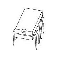
TDA1308/N2 NXP Semiconductors, TDA1308/N2 Datasheet - Page 15

TDA1308/N2
Manufacturer Part Number
TDA1308/N2
Description
Audio Amplifiers HEADPHONE DRIVER; LV
Manufacturer
NXP Semiconductors
Datasheet
1.TDA1308N2.pdf
(19 pages)
Specifications of TDA1308/N2
Product
Class-AB
Output Power
80 mW
Available Set Gain
70 dB
Thd Plus Noise
0.03 %
Operating Supply Voltage
5 V
Supply Current
3 mA
Maximum Power Dissipation
25 mW
Maximum Operating Temperature
+ 85 C
Mounting Style
Through Hole
Audio Load Resistance
32 Ohms
Dual Supply Voltage
+/- 2.5 V
Input Bias Current (max)
0.00001 uA
Input Offset Voltage
10 mV
Input Signal Type
Differential
Minimum Operating Temperature
- 40 C
Output Signal Type
Single
Supply Type
Single or Dual
Supply Voltage (max)
7 V
Supply Voltage (min)
3 V
Output Type
2-Channel Stereo
Package / Case
PDIP-8
Operational Class
Class-AB
Audio Amplifier Output Configuration
2-Channel Stereo
Audio Amplifier Function
Headphone
Total Harmonic Distortion
0.03@32Ohm%
Single Supply Voltage (typ)
5V
Dual Supply Voltage (typ)
±2.5V
Supply Current (max)
5@5VmA
Power Supply Requirement
Single/Dual
Power Dissipation
25mW
Unity Gain Bandwidth Product (typ)
5.5MHz
Rail/rail I/o Type
No
Power Supply Rejection Ratio
90dB
Single Supply Voltage (min)
3V
Single Supply Voltage (max)
7V
Dual Supply Voltage (min)
±1.5V
Dual Supply Voltage (max)
±3.5V
Operating Temp Range
-40C to 85C
Operating Temperature Classification
Industrial
Mounting
Through Hole
Pin Count
8
Package Type
PDIP
Lead Free Status / RoHS Status
Lead free / RoHS Compliant
Other names
TDA1308/N2,112
Available stocks
Company
Part Number
Manufacturer
Quantity
Price
NXP Semiconductors
TDA1308_A_4
Product data sheet
14.4 Reflow soldering
Key characteristics in reflow soldering are:
Table 8.
Table 9.
Moisture sensitivity precautions, as indicated on the packing, must be respected at all
times.
Studies have shown that small packages reach higher temperatures during reflow
soldering, see
Package thickness (mm)
< 2.5
Package thickness (mm)
< 1.6
1.6 to 2.5
> 2.5
•
•
•
2.5
Lead-free versus SnPb soldering; note that a lead-free reflow process usually leads to
higher minimum peak temperatures (see
reducing the process window
Solder paste printing issues including smearing, release, and adjusting the process
window for a mix of large and small components on one board
Reflow temperature profile; this profile includes preheat, reflow (in which the board is
heated to the peak temperature) and cooling down. It is imperative that the peak
temperature is high enough for the solder to make reliable solder joints (a solder paste
characteristic). In addition, the peak temperature must be low enough that the
packages and/or boards are not damaged. The peak temperature of the package
depends on package thickness and volume and is classified in accordance with
Table 8
SnPb eutectic process (from J-STD-020C)
Lead-free process (from J-STD-020C)
and
Figure
9
16.
Rev. 04 — 25 January 2007
Package reflow temperature ( C)
Volume (mm
< 350
235
220
Package reflow temperature ( C)
Volume (mm
< 350
260
260
250
3
3
)
)
TDA1308; TDA1308A
Figure
350 to 2000
260
250
245
Class-AB stereo headphone driver
16) than a PbSn process, thus
220
220
350
> 2000
260
245
245
© NXP B.V. 2007. All rights reserved.
15 of 19


