STA501 STMicroelectronics, STA501 Datasheet
STA501
Specifications of STA501
Available stocks


Related parts for STA501


STA501 Summary of contents
Page 1
... CMOS COMPATIBLE LOGIC INPUTS THERMAL PROTECTION THERMAL WARNING OUTPUT UNDER VOLTAGE PROTECTION DESCRIPTION STA501 is a monolithic dual half bridge stage in Mul- tipower BCD Technology. The device is particularly designed to make the out- put stage of a mono All-Digital High Efficiency AUDIO APPLICATION CIRCUIT ...
Page 2
... STA501 PIN FUNCTION N° Pin 1 GND-SUB Substrate ground Vcc Sign Signal Positive Supply 15 Vcc Positive Supply 12 Vcc Positive Supply 7 Vcc Positive Supply 4 Vcc Positive Supply 14 GND Negative Supply 13 GND Negative Supply 6 GND Negative Supply 5 GND Negative Supply N. N. OUTA Output half bridge 2 ...
Page 3
... D02AU1449 IC -STATUS Fault detected (Short circuit, or Thermal ..) Normal Operation All powers in Hi-Z state Normal operation Low absorpion Normal operation Temperature of the IC =130C Normal operation 1 GND-SUB 2 OUTB 3 OUTB GND 6 GND OUTA 9 OUTA 10 N GND 14 GND N.C. 17 N.C. 18 N.C. STA501 3/8 ...
Page 4
... STA501 ABSOLUTE MAXIMUM RATINGS Symbol V DC Supply Voltage (Pin 4,7,12,15 Maximum Voltage on pins max T Operating Temperature Range Storage and Junction Temperature stg j THERMAL DATA Symbol T Thermal Resistance Junction to Case (thermal pad) j-case T Thermal shut-down junction temperature jSD T Thermal warning temperature warn ...
Page 5
... Pin voltage = 0.3V Ibias = 3.3V Ibias = 3.3V Ibias = 3.3V PWRDN = 0 Vpin = 3.3V Vcc=30V; Tri-state=0 Input pulse width = 50% Duty; Switching Frequency = 384Khz filters; No Load Unit INB OFF OFF 0 OFF OFF 1 OFF OFF STA501 Min. Typ. Max. Unit 0 150 ns OUTPUT Q3 Q4 ...
Page 6
... STA501 Figure 1. Test Circuit. Low current dead time = MAX(DTr,DTf) Duty cycle = 50% INY Figure 2. INA Figure 3. High Current Dead time for Bridge application = ABS(DTout(A)-DTin(A))+ABS(DTOUT(B)-DTin(B)) Duty cycle=A M58 Q1 DTin(A) OUTA INA M57 Q3 Duty cycle A and B: Fixed to have DC output current of 3.5A in the direction shown in figure ...
Page 7
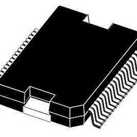
... Mold flash or protusions shall not exceed 0.15mm (0.006”) (2) No intrusion allowed inwards the leads. inch TYP. MAX. 0.138 0.13 0.039 0.008 0 0.003 0.015 0.012 0.630 0.38 0.039 0.57 0.437 0.114 0.244 1.259 0.026 0.435 0 0.003 0.625 0.043 0.043 PowerSO36 (SLUG UP) STA501 OUTLINE AND MECHANICAL DATA 7183931 7/8 ...
Page 8
... STA501 Information furnished is believed to be accurate and reliable. However, STMicroelectronics assumes no responsibility for the consequences of use of such information nor for any infringement of patents or other rights of third parties which may result from its use. No license is granted by implication or otherwise under any patent or patent rights of STMicroelectronics. Specifications mentioned in this publication are subject to change without notice ...