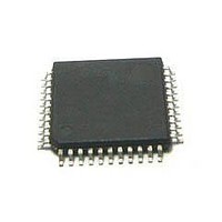
TDA7310 STMicroelectronics, TDA7310 Datasheet - Page 10

TDA7310
Manufacturer Part Number
TDA7310
Description
Audio DSPs Serial Audio Proc
Manufacturer
STMicroelectronics
Datasheet
1.TDA7310.pdf
(15 pages)
Specifications of TDA7310
Mounting Style
SMD/SMT
Package / Case
PQFP-44
Lead Free Status / RoHS Status
Lead free / RoHS Compliant
Available stocks
Company
Part Number
Manufacturer
Quantity
Price
TDA7310
APPLICATION INFORMATION (continued)
SERIAL BUS INTERFACE
S-BUS Interface and I
Data transmission from microprocessor to the
TDA7310 and viceversa takes place thru the 3-
wire S-BUS interface, consisting of the three lines
SDA, SCL, SEN. If SDA and SEN inputs are
short-circuited together, then the TDA7310 ap-
pears as a standard I
According to I
lines are connected to a positive supply voltage
via pull-up resistors.
Data Validity
As shown in fig. 15, the data on the SDA line
must be stable during the high period of the clock.
The HIGH and LOW state of the data line can
only change when the clock signal on the SCL
line is LOW.
Start and Stop Conditions
I
as shown in fig. 16 a start condition is a HIGH to
LOW transition of the SDA line while SCL is
HIGH. The stop condition is a LOW to HIGH tran-
sition of the SDA line while SCL is HIGH.
S-bus:
the start/stop conditions (points 1 and 6) are de-
tected exclusively by a transition of the SEN line
(1
level.
The SDA line is only allowed to change during the
time the SCL line is low (points 2, 3, 4, 5). after
the start information (point 1) the SEN line returns
to the HIGH level and remains uncharged for all
the time the transmission is performed.
Byte Fornat
Every byte transferred on the SDA line must con-
tain 8 bits. Each byte must be followed by an ac-
knowledge bit. The MSB is transferred first.
Acknowledge
The master ( P) puts a resistive HIGH level on
Figure 17: Acknowledge on the I
10/15
2
CBUS:
0 / 0
1)wile the SCL line is at the HIGH
2
CBUS specification the S-BUS
2
2
CBUS slave.
CBUS Compability
2
CBUS
Figure 15: Data Validity on the I
Figure 16: Timing Diagram of S-BUS and I
the SDA line during the acknowledge clock pulse
(see fig. 17). The peripheral (audioprocessor) that
acknowledges has to pull-down (LOW) the SDA
line during the acknowledge clock pulse, so that
the SDA line is stable LOW during this clock.
2
CBUS
2
CBUS


