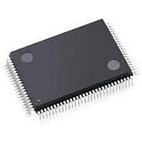
ISPPAC-CLK5510V-01T48C Lattice, ISPPAC-CLK5510V-01T48C Datasheet - Page 17

ISPPAC-CLK5510V-01T48C
Manufacturer Part Number
ISPPAC-CLK5510V-01T48C
Description
Clock Drivers & Distribution PROGRAMMABLE CLOCK GENERATOR
Manufacturer
Lattice
Datasheet
1.PAC-SYSTEMCLK5520.pdf
(48 pages)
Specifications of ISPPAC-CLK5510V-01T48C
Minimum Operating Temperature
0 C
Mounting Style
SMD/SMT
Maximum Operating Temperature
70 C
Package / Case
TQFP-100
Lead Free Status / RoHS Status
Lead free / RoHS Compliant
Available stocks
Company
Part Number
Manufacturer
Quantity
Price
Company:
Part Number:
ISPPAC-CLK5510V-01T48C
Manufacturer:
Lattice Semiconductor Corporation
Quantity:
10 000
Lattice Semiconductor
chosen to provide maximum loop stability while still providing exceptional jitter performance. Please note that when
the skew mode is set to ‘coarse’, the effective value of NxV must be doubled. Refer to the section titled ‘Coarse
Skew Mode’ on page 30 for more details.
The PLL’s loop bandwidth is a function of both the divider configuration and the loop filter settings. Figure 12 shows
the loop bandwidth as a function of the total feedback division ratio (N x V
in this plot, the PLL loop filter was set to the corresponding value recommended in Table 2. The use of non-recom-
mended loop filter settings may result in significantly different bandwidths for a given NxV divider setting.
Figure 12. PLL Loop Bandwidth vs. Feedback Divider Setting (nominal)
VCO
The ispClock5500 provides an internal VCO which provides an output frequency ranging from 320MHz to 640MHz.
The VCO is implemented using differential circuit design techniques which minimize the influence of power supply
noise on measured output jitter. The VCO is also used to generate skews as a function of the total VCO period.
Using the VCO as the basis for controlling output skew allows for highly precise and consistent skew generation,
both from device-to-device, as well as channel-to-channel within the same device.
M, N, and V Dividers
The ispClock5500 incorporates a set of programmable dividers which provide the ability to synthesize output fre-
quencies differing from that of the reference clock input.
The input, or M, divider prescales the input reference frequency, and can be programmed with integer values over
the range of 1 to 32. To achieve low levels of output jitter, it is best to use the smallest M divider value possible.
The feedback, or N, divider prescales the feedback frequency and like the M divider, can also be programmed with
integer values ranging from 1 to 32.
Each one of the five output, or V, dividers can be independently programmed to provide even division ratios ranging
from 2 to 64.
When the PLL is selected (PLL_BYPASS=LOW) and locked, the output frequency of each V divider (f
culated as:
1.75
1.25
0.75
0.25
1.5
0.5
0
1
2
0
*loop filter configured to recommended setting
Feedback Divider Setting* (Typical)
N x V Feedback Division Product
f
k
PLL Loop Bandwidth vs.
16
=
f
ref
17
N x V
M x V
32
fbk
k
48
ispClock5500 Family Data Sheet
FBK
). For each NxV feedback divider point
64
k
) may be cal-
(1)


