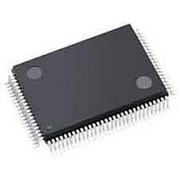
ISPPAC-CLK5510V-01T48C Lattice, ISPPAC-CLK5510V-01T48C Datasheet - Page 36

ISPPAC-CLK5510V-01T48C
Manufacturer Part Number
ISPPAC-CLK5510V-01T48C
Description
Clock Drivers & Distribution PROGRAMMABLE CLOCK GENERATOR
Manufacturer
Lattice
Datasheet
1.PAC-SYSTEMCLK5520.pdf
(48 pages)
Specifications of ISPPAC-CLK5510V-01T48C
Minimum Operating Temperature
0 C
Mounting Style
SMD/SMT
Maximum Operating Temperature
70 C
Package / Case
TQFP-100
Lead Free Status / RoHS Status
Lead free / RoHS Compliant
Available stocks
Company
Part Number
Manufacturer
Quantity
Price
Company:
Part Number:
ISPPAC-CLK5510V-01T48C
Manufacturer:
Lattice Semiconductor Corporation
Quantity:
10 000
Lattice Semiconductor
IEEE Standard 1149.1 Interface (JTAG)
Serial Port Programming Interface Communication with the ispClock5500 is facilitated via an IEEE 1149.1 test
access port (TAP). It is used by the ispClock5500 both as a serial programming interface, and for boundary scan
test purposes. A brief description of the ispClock5500 JTAG interface follows. For complete details of the reference
specification, refer to the publication, Standard Test Access Port and Boundary-Scan Architecture, IEEE Std.
1149.1-1990 (which now includes IEEE Std. 1149.1a-1993).
Overview
An IEEE 1149.1 test access port (TAP) provides the control interface for serially accessing the digital I/O of the
ispClock5500. The TAP controller is a state machine driven with mode and clock inputs. Given in the correct
sequence, instructions are shifted into an instruction register which then determines subsequent data input, data
output, and related operations. Device programming is performed by addressing the configuration register, shifting
data in, and then executing a program configuration instruction, after which the data is transferred to internal
E
are defined that access all data registers and perform other internal control operations. For compatibility between
compliant devices, two data registers are mandated by the IEEE 1149.1 specification. Others are functionally spec-
ified, but inclusion is strictly optional. Finally, there are provisions for optional data registers defined by the manu-
facturer. The two required registers are the bypass and boundary-scan registers. Figure 32 shows how the
instruction and various data registers are organized in an ispClock5500.
Figure 32. ispClock5500 TAP Registers
TAP Controller Specifics
The TAP is controlled by the Test Clock (TCK) and Test Mode Select (TMS) inputs. These inputs determine whether
an Instruction Register or Data Register operation is performed. Driven by the TCK input, the TAP consists of a
small 16-state controller design. In a given state, the controller responds according to the level on the TMS input as
shown in Figure 33. Test Data In (TDI) and TMS are latched on the rising edge of TCK, with Test Data Out (TDO)
becoming valid on the falling edge of TCK. There are six steady states within the controller: Test-Logic-Reset, Run-
2
CMOS cells. It is these non-volatile cells that store the configuration or the ispClock5500. A set of instructions
TDI
TEST ACCESS PORT (TAP)
INSTRUCTION REGISTER (8 BITS)
ADDRESS REGISTER (10 BITS)
TCK
IDCODE REGISTER (32 BITS)
B-SCAN REGISTER (56 BITS)
BYPASS REGISTER (1 BIT)
DATA REGISTER (90 BITS)
UES REGISTER (32 BITS)
LOGIC
TMS
36
OUTPUT
LATCH
TDO
ispClock5500 Family Data Sheet
NON-VOLATILE
MEMORY
E
2
CMOS


