PCK2001MDB NXP Semiconductors, PCK2001MDB Datasheet - Page 2
PCK2001MDB
Manufacturer Part Number
PCK2001MDB
Description
Clock Buffer PII CLCK DRVR MOBILE
Manufacturer
NXP Semiconductors
Datasheet
1.PCK2001MDB118.pdf
(14 pages)
Specifications of PCK2001MDB
Mounting Style
SMD/SMT
Package / Case
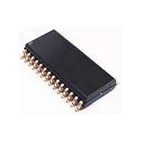
SOT-341
Lead Free Status / RoHS Status
Lead free / RoHS Compliant
Other names
PCK2001MDB,112
Available stocks
Company
Part Number
Manufacturer
Quantity
Price
Company:

Part Number:
PCK2001MDB
Manufacturer:
PHILIPS
Quantity:
40
Part Number:
PCK2001MDB
Manufacturer:
NXP/恩智浦
Quantity:
20 000


FEATURES
QUICK REFERENCE DATA
ORDERING INFORMATION
PIN CONFIGURATION
Intel and Pentium are registered trademarks of Intel Corporation.
I
2
Philips Semiconductors
2000 May 17
C is a trademark of Philips Semiconductors Corporation.
Mobile (reduced pincount) version of PCK2001
Typically used to support two SDRAM DIMMs
28-pin SSOP package
Same general features as PCK2001
See PCK2001 for 48-pin 1-18 buffer part supporting up to
4 SDRAM DIMMs
Optimized for 66 MHz, 100 MHz and 133 MHz operation
14.318–150 MHz I
SYMBOL
28-Pin Plastic SSOP
I
t
t
CC
PLH
PHL
t
t
r
f
PACKAGES
BUF_OUT16
BUF_OUT0
BUF_OUT2
BUF_OUT3
BUF_OUT1
Propagation delay
BUF_IN to BUF_OUT
Rise time
Fall time
Total supply current
BUF_IN
V
V
V
DDI2C
V
V
V
V
SDA
DD1
SS0
DD4
DD0
SS1
SS4
10
11
12
13
14
1
2
3
4
5
6
7
8
9
TOP VIEW
PARAMETER
2
C 1:10 clock buffer
TEMPERATURE RANGE
n
28
27
26
25
24
23
22
21
20
19
18
17
16
15
SA00447
0 C to +70 C
V
BUF_OUT15
BUF_OUT14
V
V
BUF_OUT13
BUF_OUT12
V
OE
V
BUF_OUT17
V
V
SCL
DD9
SS9
DD8
SS8
DD5
SS5
SSI2C
V
V
V
V
CC
CC
CC
CC
= 3.3 V, CL = 30 pF
= 3.3 V, CL = 30 pF
= 3.3 V, CL = 20 pF
= 3.465 V
2
DESCRIPTION
The PCK2001M is a 1–10 fanout buffer used for 133/100 MHz CPU,
66/33 MHz PCI, 14.318 MHz REF, or 133/100/66 MHz SDRAM
clock distribution. 10 outputs are typically used to support up to
2 SDRAM DIMMs commonly found in laptop or mobile applications.
The PCK2001M has the same features and operating characteristics
of the PCK2001 and is available in the SSOP 28 pin package.
PIN DESCRIPTION
22, 23, 26,
NUMBER
19, 24, 28
17, 21, 25
175 ps skew outputs
Individual clock output enable/disable via I
2, 3, 6, 7
1, 5, 10,
4, 8, 12,
11, 18
PIN
27
20
14
15
13
16
9
CONDITIONS
ORDER CODE
PCK2001M DB
Output
Output
Output
TYPE
Input
Input
Input
Input
Input
Input
Input
I/O
I/O
V
V
DD (0, 1, 4, 5, 8, 9)
SS (0, 1, 4, 5, 8, 9)
BUF_OUT
BUF_OUT
BUF_OUT
SYMBOL
(12–15)
(16–17)
BUF_IN
V
V
(0–3)
SDA
SCL
DDI2C
DDI2C
OE
DRAWING NUMBER
TYPICAL
Buffered clock outputs
Buffered clock outputs
Buffered clock outputs
Buffered clock input
Active high ouput enable
I
I
3.3 V power supply
Ground
3.3 V I
I
2
2
2
2
C serial data
C serial clock
C ground
PCK2001M
C
Product specification
700
2.5
2.5
1.0
50
SOT341–1
FUNCTION
2
C power supply
853-2120 23685
UNIT
ns
ns
ps
A
Related parts for PCK2001MDB
Image
Part Number
Description
Manufacturer
Datasheet
Request
R

Part Number:
Description:
14.318-150 Mhz I2c 1 18 Clock Buffer
Manufacturer:
NXP Semiconductors
Datasheet:
Part Number:
Description:
NXP Semiconductors designed the LPC2420/2460 microcontroller around a 16-bit/32-bitARM7TDMI-S CPU core with real-time debug interfaces that include both JTAG andembedded trace
Manufacturer:
NXP Semiconductors
Datasheet:

Part Number:
Description:
NXP Semiconductors designed the LPC2458 microcontroller around a 16-bit/32-bitARM7TDMI-S CPU core with real-time debug interfaces that include both JTAG andembedded trace
Manufacturer:
NXP Semiconductors
Datasheet:
Part Number:
Description:
NXP Semiconductors designed the LPC2468 microcontroller around a 16-bit/32-bitARM7TDMI-S CPU core with real-time debug interfaces that include both JTAG andembedded trace
Manufacturer:
NXP Semiconductors
Datasheet:
Part Number:
Description:
NXP Semiconductors designed the LPC2470 microcontroller, powered by theARM7TDMI-S core, to be a highly integrated microcontroller for a wide range ofapplications that require advanced communications and high quality graphic displays
Manufacturer:
NXP Semiconductors
Datasheet:
Part Number:
Description:
NXP Semiconductors designed the LPC2478 microcontroller, powered by theARM7TDMI-S core, to be a highly integrated microcontroller for a wide range ofapplications that require advanced communications and high quality graphic displays
Manufacturer:
NXP Semiconductors
Datasheet:
Part Number:
Description:
The Philips Semiconductors XA (eXtended Architecture) family of 16-bit single-chip microcontrollers is powerful enough to easily handle the requirements of high performance embedded applications, yet inexpensive enough to compete in the market for hi
Manufacturer:
NXP Semiconductors
Datasheet:
Part Number:
Description:
The XA-S3 device is a member of Philips Semiconductors? XA(eXtended Architecture) family of high performance 16-bitsingle-chip microcontrollers
Manufacturer:
NXP Semiconductors
Datasheet:

Part Number:
Description:
The NXP BlueStreak LH75401/LH75411 family consists of two low-cost 16/32-bit System-on-Chip (SoC) devices
Manufacturer:
NXP Semiconductors
Datasheet:
Part Number:
Description:
The NXP LPC3130/3131 combine an 180 MHz ARM926EJ-S CPU core, high-speed USB2
Manufacturer:
NXP Semiconductors
Datasheet:
Part Number:
Description:
The NXP LPC3141 combine a 270 MHz ARM926EJ-S CPU core, High-speed USB 2
Manufacturer:
NXP Semiconductors
Part Number:
Description:
The NXP LPC3143 combine a 270 MHz ARM926EJ-S CPU core, High-speed USB 2
Manufacturer:
NXP Semiconductors

Part Number:
Description:
The NXP LPC3152 combines an 180 MHz ARM926EJ-S CPU core, High-speed USB 2
Manufacturer:
NXP Semiconductors
Part Number:
Description:
The NXP LPC3154 combines an 180 MHz ARM926EJ-S CPU core, High-speed USB 2
Manufacturer:
NXP Semiconductors