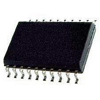
HV430WG Supertex, HV430WG Datasheet - Page 8

HV430WG
Manufacturer Part Number
HV430WG
Description
Telephone Ringers Hv Ring Gen
Manufacturer
Supertex
Type
Multipler
Datasheet
1.HV430WG-G.pdf
(9 pages)
Specifications of HV430WG
Function
Telecom Ringer
Mounting Style
SMD/SMT
Operating Supply Voltage
2.7 V to 5.25 V
Product
Telecom Ringer
Package / Case
SOIC-20 Wide
Maximum Operating Temperature
+ 85 C
Minimum Operating Temperature
- 40 C
Primary Target Application
Generator Circuit
Lead Free Status / RoHS Status
Lead free / RoHS Compliant
Pin Description
Pin #
10
12
13
14
15
16
17
18
19
20
11
1
2
3
4
5
6
7
8
9
DEADBAND
VNGATE
VPGATE
ENABLE
VNSEN
VPSEN
RESET
FAULT
MODE
SGND
PGND
Name
VNN2
VNN1
VPP1
VPP2
Supertex inc.
VDD
PIN
NIN
N/C
Description
Logic supply voltage.
Logic output. Fault is at logic low when either current limit sense pin, VPSEN or VNSEN, is acti-
vated. Remains active until overcurrent condition clears or ENABLE = 0 or RESET = 0.
Logic mode input. 0 = single-control; 1 = dual-control. When MODE is high, NIN and PIN inde-
pendently control N
complementary manner. (See Truth Table)
Logic control input. When mode is high, logic input high turns on the external high voltage P-chan-
nel MOSFET. Internally pulled low.
Logic control input. When mode is high, logic input high turns on the external high voltage N-chan-
nel MOSFET. Internally pulled low.
Logic enable input. Logic high enables IC. Internally pulled low.
Power-on reset. A capacitor connected between this pin and ground determines the delay time
between application of VDD and when the device outputs are enabled. Low leakage tantalum
recommended.
A resistor between this pin and ground sets the ‘break-before-make’ time between output transi-
tions. Applicable only in single-control mode. For minimum deadtime, a 5.6kΩ resistor to ground
should be used. For dual-input mode, tie to VDD.
Low voltage logic ground.
High voltage logic ground.
Negative gate voltage supply. Generated by an internal linear regulator. A 25V, 100nF capacitor
should beconnected between VNN2 and VNN1.
Negative high voltage supply.
Pulse by pulse over current sensing for N-Channel MOSFET.
Gate drive for external N-channel MOSFET.
No connect.
Gate drive for external P-channel MOSFET.
Pulse by pulse over current sensing for P-Channel MOSFET.
Positive high voltage supply.
Positive gate voltage supply. Generated by an internal linear regulator. A 25V, 100nF capacitor
should beconnected between VPP2 and VPP1.
●
1235 Bordeaux Drive, Sunnyvale, CA 94089
OUT
and P
OUT
, respectively. When MODE is low, NIN controls both outputs in a
8
●
Tel: 408-222-8888
●
www.supertex.com
HV430


