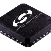
SI5023-BMR Silicon Laboratories Inc, SI5023-BMR Datasheet - Page 14

SI5023-BMR
Manufacturer Part Number
SI5023-BMR
Description
Telecom Line Management ICs SNT/SDH GbE 2.7Gbps OC48/12/3 STM16/4/1
Manufacturer
Silicon Laboratories Inc
Type
Evaluation Board For Si5023 Siphy Multi-Rate Sonet/ Sth Clock and Data Recovery ICr
Datasheet
1.SI5023-EVB.pdf
(28 pages)
Specifications of SI5023-BMR
Mounting Style
SMD/SMT
Package / Case
MLP-28
Lead Free Status / RoHS Status
Lead free / RoHS Compliant
Si5023
LOS signal hysteresis for the Si5023 CDR. The value of
R1 may be chosen to provide a range of hysteresis from
3 to 8 dB where a nominal value of 800 Ω adjusts the
hysteresis level to approximately 6 dB. Use a value of
500 Ω or 1000 Ω for R1 to provide 3 dB or 8 dB of
hysteresis, respectively.
Hysteresis is defined as the ratio of the LOS deassert
level (LOSD) and the LOS assert level (LOSA). The
hysteresis in decibels is calculated as 20log(LOSD/
LOSA).
14
Figure 6. LOS_LVL Mapping (PRBS23 Data)
Set LOS
40 mV
30 mV
15 mV
Level
0 mV
Figure 7. LOS Signal Hysteresis
R1
R2
0 V
10k
1.00 V
3
LOS_LVL
LOS_LVL (V)
Si5023
1.50 V
CDR
LOS
LOS Limited by Device Noise
1.875 V
40mV/V
9
2.25 V
LOS Alarm
2.50 V
10 mV
max
Rev. 1.3
4.9. Bit Error Rate (BER) Detection
The Si5023 uses a proprietary Silicon Laboratories
algorithm to generate a BER alarm on the BER_ALM
pin and a BER indicator on the BERMON pin.
The BERMON output is always enabled and functions
as a dynamic analog level that is proportional to the
detected bit error rate. This BERMON indicator can be
used to monitor the quality and error status on the
receive data input channel. The range of operation of
the BER processor is between 1E-09 to 1E-03 as
shown in Figures 8, 9, and 10. It is recommended that
the BERMON output be filtered with an active low-pass
filter configuration as shown in Figure 11. The external
LPF may be followed by a voltage comparator or
analog-to-digital converter where constant channel
monitoring is desired.
4.10. Data Slicing Level
The Si5023 provides the ability to externally adjust the
slicing
optimization. Adjustments in slicing level of ±25 mV
(typical, relative to the internally-set input common
mode voltage) are supported. The slicing level is set by
applying a voltage between 0.75 V and 2.25 V to the
SLICE_LVL input. See Figures 12 and 13 for the
operation levels of the slice circuit.
When SLICE_LVL is driven below 500 mV, the slicing
level adjustment is disabled, and the slicing level is set
to the cross-point of the differential input signal.
Note: The slice circuit is designed to only work with pseudo-
4.11. PLL Performance
The PLL implementation used in the Si5023 is fully-
compliant with the jitter specifications proposed for
SONET/SDH equipment by Bellcore GR-253-CORE,
Issue 3, September 2000 and ITU-T G.958.
4.11.1. Jitter Tolerance
The Si5023’s tolerance to input jitter exceeds that of the
Bellcore/ITU mask shown in Figure 14. This mask
defines the level of peak-to-peak sinusoidal jitter that
must be tolerated when applied to the differential data
input of the device.
Note: There are no entries in the mask table for the data rate
random, dc-balanced data.
corresponding to OC-24 as that rate is not specified by
either GR-253 or G.958.
level
for
applications
that
require
BER


