RTU002P02T106 Rohm Semiconductor, RTU002P02T106 Datasheet
Home Discrete Semiconductor Products MOSFETs, GaNFETs - Single RTU002P02T106
Manufacturer Part Number
RTU002P02T106
Description
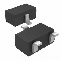
MOSFET P-CH 20V 250MA SOT-323
Manufacturer
Rohm Semiconductor
Specifications of RTU002P02T106
Fet Type
MOSFET P-Channel, Metal Oxide
Fet Feature
Standard
Rds On (max) @ Id, Vgs
1.5 Ohm @ 250mA, 4.5V
Drain To Source Voltage (vdss)
20V
Current - Continuous Drain (id) @ 25° C
250mA
Vgs(th) (max) @ Id
2V @ 1mA
Input Capacitance (ciss) @ Vds
50pF @ 10V
Power - Max
200mW
Mounting Type
Surface Mount
Package / Case
SC-70-3, SOT-323-3
Transistor Polarity
P Channel
Drain Source Voltage Vds
-20V
On Resistance Rds(on)
1ohm
Rds(on) Test Voltage Vgs
-4.5V
Voltage Vgs Max
-12V
Transistor Case Style
SOT-323
No. Of Pins
3
Svhc
No SVHC
Configuration
Single
Resistance Drain-source Rds (on)
1.5 Ohm @ 4.5 V
Drain-source Breakdown Voltage
20 V
Gate-source Breakdown Voltage
+/- 12 V
Continuous Drain Current
0.25 A
Power Dissipation
200 mW
Mounting Style
SMD/SMT
Lead Free Status / RoHS Status
Lead free / RoHS Compliant
Gate Charge (qg) @ Vgs
-
Lead Free Status / Rohs Status
Lead free / RoHS Compliant
Other names
RTU002P02T106TR
Available stocks
Part Number:
RTU002P02T106
Transistors
2.5V Drive Pch MOS FET
RTU002P02
Silicon P-channel MOS FET
1) Low On-resistance.
2) Low voltage drive (2.5V drive).
Switching
∗1 Pw≤10µs, Duty cycle≤1%
∗2 Each terminal mounted on a recommended land
∗ Each terminal mounted on a recommended land
Channel to ambient
Drain-source voltage
Gate-source voltage
Drain current
Total power dissipation
Channel temperature
Range of storage temperature
Type
RTU002P02
Structure
Features
Applications
Package specifications
Absolute maximum ratings (Ta=25°C)
Thermal resistance
Package
Code
Basic ordering unit (pieces)
Parameter
Parameter
Continuous
Pulsed
Taping
T106
3000
Rth(ch-a)
Symbol
Symbol
V
V
Tstg
Tch
I
P
DSS
GSS
I
DP
D
D
∗1
∗2
∗
−55 to +150
Limits
Limits
±0.25
±0.5
625
−20
±12
150
0.2
∗1 ESD PROTECTION DIODE
∗2 BODY DIODE
Inner circuit
(1) Source
(2) Gate
(3) Drain
External dimensions (Unit : mm)
UMT3
°C/W
(2)
Unit
Unit
°C
°C
W
V
V
A
A
∗1
Abbreviated symbol : TW
0.65
( 3 )
( 2 )
1.3
2.0
0.65
0.3
(3)
(1)
( 1 )
∗2
Each lead has same dimensions
0.2
0.15
RTU002P02
0.9
0.7
(1) Source
(2) Gate
(3) Drain
1/2
Related parts for RTU002P02T106
RTU002P02T106 Summary of contents
Transistors 2.5V Drive Pch MOS FET RTU002P02 Structure Silicon P-channel MOS FET Features 1) Low On-resistance. 2) Low voltage drive (2.5V drive). Applications Switching Package specifications Package Taping Type Code T106 Basic ordering unit (pieces) 3000 RTU002P02 Absolute maximum ratings ...
Transistors Electrical characteristics (Ta=25°C) Parameter Symbol Gate-source leakage I GSS Drain-source breakdown voltage V (BR) DSS Zero gate voltage drain current I DSS Gate threshold voltage V GS (th) Static drain-source on-state R DS (on) resistance Forward transfer admittance Y ...
Appendix No technical content pages of this document may be reproduced in any form or transmitted by any means without prior permission of ROHM CO.,LTD. The contents described herein are subject to change without notice. The specifications for the product ...
Related keywords
rtu002p02 RTU002P02T106 datasheet RTU002P02T106 data sheet RTU002P02T106 pdf datasheet RTU002P02T106 component RTU002P02T106 part RTU002P02T106 distributor RTU002P02T106 RoHS RTU002P02T106 datasheet download