IXTA160N10T7 IXYS, IXTA160N10T7 Datasheet
IXTA160N10T7
Specifications of IXTA160N10T7


Related parts for IXTA160N10T7


IXTA160N10T7 Summary of contents
Page 1
... D = ± GSS DSS DS DSS Notes 1 DS(on © 2006 IXYS CORPORATION All rights reserved Preliminary Technical Information IXTA160N10T7 Maximum Ratings 100 = 1 MΩ 100 GS ± 30 160 120 430 JM 25 500 ≤ DSS 430 -55 ... +175 175 -55 ... +175 300 260 3 Characteristic Values Min. Typ. ...
Page 2
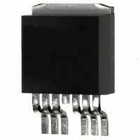
... A 37 DSS D 40 Characteristic Values Min. Typ. JM 100 The Technical Specifications 4,931,844 5,049,961 5,237,481 6,162,665 5,017,508 5,063,307 5,381,025 6,259,123 B1 5,034,796 5,187,117 5,486,715 6,306,728 B1 IXTA160N10T7 TO-263 (7-lead) (IXTA...7) Outline Max Pins Gate Source 4 - Drain 0.35 °C/W 5,6,7 - Source Tab (8) - Drain Max. 160 A 430 A 1 ...
Page 3
... 0 10V 1.6 2 2.4 2.8 = 80A Value D 140 120 T = 175ºC J 100 T = 25ºC J 200 250 300 IXTA160N10T7 Fig. 2. Extended Output Characteristics @ 25ºC 300 V = 10V GS 275 9V 250 8V 225 200 175 7V 150 125 100 Volts DS Fig Normalized to I DS(on) vs. Junction Temperature 2 ...
Page 4
... T = 25º 1.1 1.2 1.3 1.4 1.00 C iss C oss 0.10 C rss 0.01 0.0001 IXTA160N10T7 Fig. 8. Transconductance 40ºC J 25ºC 150º 100 120 140 I - Amperes D Fig. 10. Gate Charge V = 50V 25A 10mA NanoCoulombs G Fig. 12. Maximum Transient Thermal Impedance 0.001 ...
Page 5
... I = 25A 140 - - - - d(off) 77 130 = 5 Ω 10V 120 V = 50V DS 71 110 68 100 25º IXTA160N10T7 Fig. 14. Resistive Turn-on Rise Time vs. Drain Current Ω 10V 50V Amperes D Fig. 16. Resistive Turn-off Switching Times vs. Junction Temperature d(off Ω 50V 25A 50A 25A 50A Degrees Centigrade J Fig ...