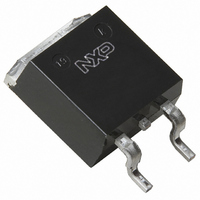
BUK9624-55A,118 NXP Semiconductors, BUK9624-55A,118 Datasheet - Page 5

BUK9624-55A,118
Manufacturer Part Number
BUK9624-55A,118
Description
MOSFET N-CH 55V 46A D2PAK
Manufacturer
NXP Semiconductors
Series
TrenchMOS™r
Specifications of BUK9624-55A,118
Package / Case
D²Pak, TO-263 (2 leads + tab)
Fet Type
MOSFET N-Channel, Metal Oxide
Fet Feature
Logic Level Gate
Rds On (max) @ Id, Vgs
21.7 mOhm @ 25A, 10V
Drain To Source Voltage (vdss)
55V
Current - Continuous Drain (id) @ 25° C
46A
Vgs(th) (max) @ Id
2V @ 1mA
Input Capacitance (ciss) @ Vds
1815pF @ 25V
Power - Max
105W
Mounting Type
Surface Mount
Minimum Operating Temperature
- 55 C
Configuration
Single
Transistor Polarity
N-Channel
Resistance Drain-source Rds (on)
0.0217 Ohm @ 10 V
Drain-source Breakdown Voltage
55 V
Gate-source Breakdown Voltage
+/- 10 V
Continuous Drain Current
46 A
Power Dissipation
105000 mW
Maximum Operating Temperature
+ 175 C
Mounting Style
SMD/SMT
Lead Free Status / RoHS Status
Lead free / RoHS Compliant
Gate Charge (qg) @ Vgs
-
Lead Free Status / Rohs Status
Lead free / RoHS Compliant
Other names
934056287118
BUK9624-55A /T3
BUK9624-55A /T3
BUK9624-55A /T3
BUK9624-55A /T3
8. Characteristics
Table 5:
T
Philips Semiconductors
9397 750 07538
Product specification
Symbol
Static characteristics
V
V
I
I
R
Dynamic characteristics
C
C
C
t
t
t
t
L
L
DSS
GSS
d(on)
r
d(off)
f
j
d
s
(BR)DSS
GS(th)
DSon
iss
oss
rss
= 25 C unless otherwise specified
Characteristics
Parameter
drain-source breakdown
voltage
gate-source threshold voltage I
drain-source leakage current
gate-source leakage current
drain-source on-state
resistance
input capacitance
output capacitance
reverse transfer capacitance
turn-on delay time
rise time
turn-off delay time
fall time
internal drain inductance
internal source inductance
Conditions
I
Figure 9
V
V
V
Figure 7
V
V
V
f = 1 MHz;
V
V
from drain lead 6mm from
package to centre of die
from contact screw on
mounting base to centre of
die SOT78
from upper edge of drain
mounting base to centre of
die SOT404
from source lead to source
bond pad
D
D
DS
GS
GS
GS
GS
GS
DD
GS
T
T
T
T
T
T
T
T
T
T
T
= 0.25 mA; V
= 1 mA; V
j
j
j
j
j
j
j
j
j
j
j
= 55 V; V
= 25 C
= 55 C
= 25 C
= 175 C
= 55 C
= 25 C
= 175 C
= 10 V; V
= 5 V; I
= 25 C
= 175 C
= 4.5 V; I
= 25 C
= 10 V; I
= 25 C
= 0 V; V
= 30 V; R
= 5 V; R
Rev. 01 — 29 September 2000
and
Figure 12
D
BUK9524-55A; BUK9624-55A
DS
DS
G
D
8
= 25 A;
D
GS
L
= 10 ;
= 25 A;
DS
= V
= 25 A;
GS
= 25 V;
= 1.2 ;
= 0 V
= 0 V
= 0 V
GS
;
Min
55
50
1
0.5
TrenchMOS™ logic level FET
Typ
1.5
0.05
2
20
19
1361
239
162
17.5
104
82.5
80
4.5
3.5
2.5
7.5
© Philips Electronics N.V. 2000. All rights reserved.
Max
2
2.3
10
500
100
24
50
26
21.7
1815
287
222
Unit
V
V
V
V
V
nA
m
m
m
m
pF
pF
pF
ns
ns
ns
ns
nH
nH
nH
nH
5 of 15
A
A


