BUK7618-55,118 NXP Semiconductors, BUK7618-55,118 Datasheet - Page 4
BUK7618-55,118
Manufacturer Part Number
BUK7618-55,118
Description
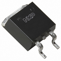
MOSFET N-CH 55V 57A SOT404
Manufacturer
NXP Semiconductors
Series
TrenchMOS™r
Specifications of BUK7618-55,118
Package / Case
D²Pak, TO-263 (2 leads + tab)
Fet Type
MOSFET N-Channel, Metal Oxide
Fet Feature
Standard
Rds On (max) @ Id, Vgs
18 mOhm @ 25A, 10V
Drain To Source Voltage (vdss)
55V
Current - Continuous Drain (id) @ 25° C
57A
Vgs(th) (max) @ Id
4V @ 1mA
Input Capacitance (ciss) @ Vds
2000pF @ 25V
Power - Max
125W
Mounting Type
Surface Mount
Minimum Operating Temperature
- 55 C
Configuration
Single
Transistor Polarity
N-Channel
Resistance Drain-source Rds (on)
0.018 Ohm @ 10 V
Drain-source Breakdown Voltage
55 V
Gate-source Breakdown Voltage
16 V
Continuous Drain Current
57 A
Power Dissipation
125000 mW
Maximum Operating Temperature
+ 175 C
Mounting Style
SMD/SMT
Lead Free Status / RoHS Status
Lead free / RoHS Compliant
Gate Charge (qg) @ Vgs
-
Lead Free Status / Rohs Status
Lead free / RoHS Compliant
Other names
934045250118
BUK7618-55 /T3
BUK7618-55 /T3
BUK7618-55 /T3
BUK7618-55 /T3
Available stocks
Company
Part Number
Manufacturer
Quantity
Price

Part Number:
BUK7618-55,118
Manufacturer:
NEXPERIA/安世
Quantity:
20 000


Philips Semiconductors
April 1998
TrenchMOS
Standard level FET
ID/A
Fig.5. Typical output characteristics, T
I
100
ID/A
D
Fig.6. Typical on-state resistance, T
80
60
40
20
30
25
20
15
10
100
0
= f(V
80
60
40
20
0
RDS(ON)/mOhm
0
10 15 20 25 30 35 40 45 50 55 60 65 70 75 80 85 90 95 100
16
10
0
Fig.7. Typical transfer characteristics.
GS
1
) ; conditions: V
R
VGS/V =
I
DS(ON)
2
D
2
= f(V
Tj/C = 175
= f(I
3
transistor
8
7.5
DS
6
); parameter V
4
D
4
); parameter V
ID/A
VSD/V
VGS/V
DS
5
25
= 25 V; parameter T
6.5
6
6
VGS/V =
7
7
GS
GS
8
j
8
j
= 25 ˚C .
8
= 25 ˚C .
7
6.5
6
5.5
5
4.5
4
9
9
10
10
10
j
4
Fig.9. Normalised drain-source on-state resistance.
gfs/S
a = R
V
35
30
25
20
15
10
Fig.8. Typical transconductance, T
2.5
1.5
0.5
-100
5
0
5
4
3
2
1
0
GS(TO)
-100
2
1
0
VGS(TO) / V
a
DS(ON)
max.
min.
typ.
g
Fig.10. Gate threshold voltage.
= f(T
fs
-50
-50
/R
= f(I
20
DS(ON)25 ˚C
j
); conditions: I
BUK959-60
D
); conditions: V
0
0
Tmb / degC
40
Tj / C
= f(T
50
50
ID/A
Rds(on) normlised to 25degC
j
); I
D
= 1 mA; V
D
60
100
100
= 25 A; V
DS
Product specification
= 25 V
BUK7618-55
150
BUK759-60
150
j
80
= 25 ˚C .
DS
GS
= V
Rev 1.000
= 5 V
200
200
GS
100
Related parts for BUK7618-55,118
Image
Part Number
Description
Manufacturer
Datasheet
Request
R

Part Number:
Description:
MOSFET Power TAPE13 PWR-MOS
Manufacturer:
NXP Semiconductors

Part Number:
Description:
NXP Semiconductors designed the LPC2420/2460 microcontroller around a 16-bit/32-bitARM7TDMI-S CPU core with real-time debug interfaces that include both JTAG andembedded trace
Manufacturer:
NXP Semiconductors
Datasheet:

Part Number:
Description:
NXP Semiconductors designed the LPC2458 microcontroller around a 16-bit/32-bitARM7TDMI-S CPU core with real-time debug interfaces that include both JTAG andembedded trace
Manufacturer:
NXP Semiconductors
Datasheet:
Part Number:
Description:
NXP Semiconductors designed the LPC2468 microcontroller around a 16-bit/32-bitARM7TDMI-S CPU core with real-time debug interfaces that include both JTAG andembedded trace
Manufacturer:
NXP Semiconductors
Datasheet:
Part Number:
Description:
NXP Semiconductors designed the LPC2470 microcontroller, powered by theARM7TDMI-S core, to be a highly integrated microcontroller for a wide range ofapplications that require advanced communications and high quality graphic displays
Manufacturer:
NXP Semiconductors
Datasheet:
Part Number:
Description:
NXP Semiconductors designed the LPC2478 microcontroller, powered by theARM7TDMI-S core, to be a highly integrated microcontroller for a wide range ofapplications that require advanced communications and high quality graphic displays
Manufacturer:
NXP Semiconductors
Datasheet:
Part Number:
Description:
The Philips Semiconductors XA (eXtended Architecture) family of 16-bit single-chip microcontrollers is powerful enough to easily handle the requirements of high performance embedded applications, yet inexpensive enough to compete in the market for hi
Manufacturer:
NXP Semiconductors
Datasheet:
Part Number:
Description:
The XA-S3 device is a member of Philips Semiconductors? XA(eXtended Architecture) family of high performance 16-bitsingle-chip microcontrollers
Manufacturer:
NXP Semiconductors
Datasheet:

Part Number:
Description:
The NXP BlueStreak LH75401/LH75411 family consists of two low-cost 16/32-bit System-on-Chip (SoC) devices
Manufacturer:
NXP Semiconductors
Datasheet:
Part Number:
Description:
The NXP LPC3130/3131 combine an 180 MHz ARM926EJ-S CPU core, high-speed USB2
Manufacturer:
NXP Semiconductors
Datasheet:
Part Number:
Description:
The NXP LPC3141 combine a 270 MHz ARM926EJ-S CPU core, High-speed USB 2
Manufacturer:
NXP Semiconductors
Part Number:
Description:
The NXP LPC3143 combine a 270 MHz ARM926EJ-S CPU core, High-speed USB 2
Manufacturer:
NXP Semiconductors

Part Number:
Description:
The NXP LPC3152 combines an 180 MHz ARM926EJ-S CPU core, High-speed USB 2
Manufacturer:
NXP Semiconductors
Part Number:
Description:
The NXP LPC3154 combines an 180 MHz ARM926EJ-S CPU core, High-speed USB 2
Manufacturer:
NXP Semiconductors