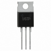
BUK9515-100A,127 NXP Semiconductors, BUK9515-100A,127 Datasheet - Page 2

BUK9515-100A,127
Manufacturer Part Number
BUK9515-100A,127
Description
MOSFET N-CH 100V 75A SOT78
Manufacturer
NXP Semiconductors
Series
TrenchMOS™r
Datasheet
1.BUK9615-100A118.pdf
(9 pages)
Specifications of BUK9515-100A,127
Fet Type
MOSFET N-Channel, Metal Oxide
Fet Feature
Logic Level Gate
Rds On (max) @ Id, Vgs
14.4 mOhm @ 25A, 10V
Drain To Source Voltage (vdss)
100V
Current - Continuous Drain (id) @ 25° C
75A
Vgs(th) (max) @ Id
2V @ 1mA
Input Capacitance (ciss) @ Vds
8600pF @ 25V
Power - Max
230W
Mounting Type
Through Hole
Package / Case
TO-220AB-3
Configuration
Single
Transistor Polarity
N-Channel
Resistance Drain-source Rds (on)
0.0144 Ohms
Drain-source Breakdown Voltage
100 V
Gate-source Breakdown Voltage
+/- 10 V
Continuous Drain Current
75 A
Power Dissipation
230 W
Maximum Operating Temperature
+ 175 C
Mounting Style
Through Hole
Minimum Operating Temperature
- 55 C
Lead Free Status / RoHS Status
Lead free / RoHS Compliant
Gate Charge (qg) @ Vgs
-
Lead Free Status / Rohs Status
Details
Other names
934055410127
BUK9515-100A
BUK9515-100A
BUK9515-100A
BUK9515-100A
Philips Semiconductors
Logic level FET
STATIC CHARACTERISTICS
T
DYNAMIC CHARACTERISTICS
T
REVERSE DIODE LIMITING VALUES AND CHARACTERISTICS
T
November 1999
TrenchMOS
j
SYMBOL PARAMETER
V
V
I
I
R
mb
SYMBOL PARAMETER
C
C
C
t
t
t
t
L
L
L
L
j
SYMBOL PARAMETER
I
I
V
t
Q
= 25˚C unless otherwise specified
DSS
GSS
d on
r
d off
f
DR
DRM
rr
= 25˚C unless otherwise specified
d
d
d
s
(BR)DSS
GS(TO)
SD
DS(ON)
iss
oss
rss
rr
= 25˚C unless otherwise specified
Drain-source breakdown
voltage
Gate threshold voltage
Zero gate voltage drain current
Gate source leakage current
Drain-source on-state
resistance
Input capacitance
Output capacitance
Feedback capacitance
Turn-on delay time
Turn-on rise time
Turn-off delay time
Turn-off fall time
Internal drain inductance
Internal drain inductance
Internal drain inductance
Internal source inductance
Continuous reverse drain
current
Pulsed reverse drain current
Diode forward voltage
Reverse recovery time
Reverse recovery charge
transistor
CONDITIONS
V
V
V
V
V
V
V
CONDITIONS
V
V
V
Measured from drain lead 6 mm
from package to centre of die
Measured from contact screw on
tab to centre of die(TO220AB)
Measured from upper edge of drain
tab to centre of die(SOT404)
Measured from source lead to
source bond pad
CONDITIONS
I
I
I
V
F
F
F
GS
DS
DS
GS
GS
GS
GS
GS
DD
GS
GS
= 25 A; V
= 75 A; V
= 75 A; -dI
= V
= 100 V; V
= 0 V; I
= 10 V; V
= 5 V; I
= 10 V; I
= 4.5 V; I
= 0 V; V
= 30 V; R
= 5 V; R
= -10 V; V
GS
; I
2
D
D
D
GS
GS
DS
G
D
F
= 0.25 mA;
= 1 mA
= 25 A
D
/dt = 100 A/ s;
load
= 10
= 0 V
= 0 V
= 25 A
R
GS
DS
= 25 V; f = 1 MHz
= 25 A
= 30 V
=1.2 ;
= 0 V;
= 0 V
T
T
T
T
T
j
j
j
j
j
= 175˚C
= 175˚C
= 175˚C
= -55˚C
= -55˚C
MIN.
MIN.
MIN.
100
0.5
89
1
-
-
-
-
-
-
-
-
-
-
-
-
-
-
-
-
-
-
-
-
-
-
-
-
-
TYP.
TYP.
6500
TYP.
0.05
11.5
0.85
0.24
550
325
130
400
130
1.5
4.5
3.5
2.5
7.5
1.1
BUK9515-100A
BUK9615-100A
12
45
60
2
-
-
-
-
-
-
-
-
-
Product specification
MAX.
MAX.
MAX.
8600
40.5
14.4
500
100
660
400
195
560
190
313
2.0
2.3
1.2
10
15
16
65
75
-
-
-
-
-
-
-
-
-
-
Rev 1.000
UNIT
UNIT
UNIT
m
m
m
m
nH
nH
nH
nH
nA
pF
pF
pF
ns
ns
ns
ns
ns
V
V
V
V
V
A
A
V
V
C
A
A


