STD5NK50Z-1 STMicroelectronics, STD5NK50Z-1 Datasheet - Page 3
STD5NK50Z-1
Manufacturer Part Number
STD5NK50Z-1
Description
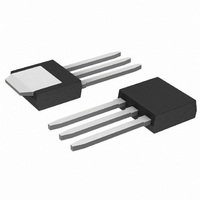
MOSFET N-CH 500V 4.4A IPAK
Manufacturer
STMicroelectronics
Series
SuperMESH™r
Datasheet
1.STD5NK50ZT4.pdf
(17 pages)
Specifications of STD5NK50Z-1
Fet Type
MOSFET N-Channel, Metal Oxide
Fet Feature
Standard
Rds On (max) @ Id, Vgs
1.5 Ohm @ 2.2A, 10V
Drain To Source Voltage (vdss)
500V
Current - Continuous Drain (id) @ 25° C
4.4A
Vgs(th) (max) @ Id
4.5V @ 50µA
Gate Charge (qg) @ Vgs
28nC @ 10V
Input Capacitance (ciss) @ Vds
535pF @ 25V
Power - Max
70W
Mounting Type
Through Hole
Package / Case
IPak, TO-251, DPak, VPak (3 straight leads + tab)
Transistor Polarity
N Channel
Continuous Drain Current Id
2.2A
Drain Source Voltage Vds
500V
On Resistance Rds(on)
1.22ohm
Rds(on) Test Voltage Vgs
10V
Threshold Voltage Vgs Typ
3.75V
Rohs Compliant
Yes
Configuration
Single
Resistance Drain-source Rds (on)
1.5 Ohms
Drain-source Breakdown Voltage
500 V
Gate-source Breakdown Voltage
+/- 30 V
Continuous Drain Current
4.4 A
Power Dissipation
70 W
Maximum Operating Temperature
+ 150 C
Mounting Style
Through Hole
Minimum Operating Temperature
- 55 C
Lead Free Status / RoHS Status
Lead free / RoHS Compliant
Available stocks
Company
Part Number
Manufacturer
Quantity
Price
Company:

Part Number:
STD5NK50Z-1
Manufacturer:
ST
Quantity:
12 500
Part Number:
STD5NK50Z-1
Manufacturer:
ST
Quantity:
20 000


ELECTRICAL CHARACTERISTICS (T
Table 7: On /Off
Table 8: Dynamic
Table 9: Source Drain Diode
(1) Pulsed: Pulse duration = 300 µs, duty cycle 1.5 %.
(2) Pulse width limited by safe operating area.
(3) C
C
V
OSS eq
Symbol
Symbol
Symbol
I
V
V
R
SDM
(BR)DSS
g
oss eq.
t
t
I
I
C
SD
I
C
GS(th)
C
Q
d(on)
d(off)
Q
DS(on
fs
RRM
DSS
GSS
I
Q
Q
SD
t
oss
t
t
iss
rss
rr
gs
gd
r
f
(1)
g
rr
(1)
(2)
(3)
is defined as a constant equivalent capacitance giving the same charging time as C
.
Drain-source Breakdown
Voltage
Zero Gate Voltage
Drain Current (V
Gate-body Leakage
Current (V
Gate Threshold Voltage
Static Drain-source On
Resistance
Forward Transconductance V
Input Capacitance
Output Capacitance
Reverse Transfer
Capacitance
Equivalent Output
Capacitance
Turn-on Delay Time
Rise Time
Turn-off-Delay Time
Fall Time
Total Gate Charge
Gate-Source Charge
Gate-Drain Charge
Source-drain Current
Source-drain Current (pulsed)
Forward On Voltage
Reverse Recovery Time
Reverse Recovery Charge
Reverse Recovery Current
Parameter
Parameter
Parameter
DS
= 0)
GS
STB5NK50Z/-1 - STD5NK50Z/-1 - STP5NK50Z - STP5NK50ZFP
= 0)
I
V
V
V
V
V
D
CASE
V
V
V
R
(see Figure 19)
V
V
(see Figure 22)
DS
DS
GS
DS
GS
DS
DS
GS
DD
DD
GS
= 1 mA, V
G
I
I
V
(see Figure 20)
SD
SD
= Max Rating
= Max Rating, T
= V
= 4.7
= ± 20 V
= 10 V, I
DD
= 25 V, f = 1 MHz, V
= 15 V , I
= 0 V, V
= 250 V, I
= 400 V, I
= 10 V
=25°C UNLESS OTHERWISE SPECIFIED)
= 4.4 A, V
= 4.4 A, di/dt = 100 A/µs
Test Conditions
Test Conditions
GS
= 30V, T
Test Conditions
, I
GS
D
D
V
DS
= 50 µA
D
GS
= 2.2 A
D
D
= 0
= 2.2 A
= 0 to 400 V
j
= 2.2 A,
= 4.4 A,
GS
= 10 V
= 150°C
C
= 0
= 125°C
GS
= 0
Min.
Min.
Min.
500
oss
3
when V
DS
1425
Typ.
Typ.
Typ.
3.75
1.22
535
310
3.1
9.2
75
17
45
15
10
32
15
20
10
increases from 0 to 80% V
4
Max.
Max.
Max.
± 10
17.6
4.5
4.4
1.6
1.5
50
28
1
Unit
Unit
Unit
nC
nC
nC
nC
µA
µA
µA
pF
pF
pF
pF
ns
ns
ns
ns
ns
3/17
V
V
S
A
A
V
A
DSS
.
Related parts for STD5NK50Z-1
Image
Part Number
Description
Manufacturer
Datasheet
Request
R

Part Number:
Description:
STMicroelectronics [RIPPLE-CARRY BINARY COUNTER/DIVIDERS]
Manufacturer:
STMicroelectronics
Datasheet:
Part Number:
Description:
STMicroelectronics [LIQUID-CRYSTAL DISPLAY DRIVERS]
Manufacturer:
STMicroelectronics
Datasheet:

Part Number:
Description:
BOARD EVAL FOR MEMS SENSORS
Manufacturer:
STMicroelectronics
Datasheet:
Part Number:
Description:
NPN TRANSISTOR POWER MODULE
Manufacturer:
STMicroelectronics
Datasheet:
Part Number:
Description:
TURBOSWITCH ULTRA-FAST HIGH VOLTAGE DIODE
Manufacturer:
STMicroelectronics
Datasheet:
Part Number:
Description:
Manufacturer:
STMicroelectronics
Datasheet:
Part Number:
Description:
DIODE / SCR MODULE
Manufacturer:
STMicroelectronics
Datasheet:
Part Number:
Description:
DIODE / SCR MODULE
Manufacturer:
STMicroelectronics
Datasheet:
Part Number:
Description:
Search -----> STE16N100
Manufacturer:
STMicroelectronics
Datasheet:
Part Number:
Description:
Search ---> STE53NA50
Manufacturer:
STMicroelectronics
Datasheet:
Part Number:
Description:
NPN Transistor Power Module
Manufacturer:
STMicroelectronics
Datasheet:
Part Number:
Description:
DIODE / SCR MODULE
Manufacturer:
STMicroelectronics
Datasheet: