STD40NF10 STMicroelectronics, STD40NF10 Datasheet
STD40NF10
Specifications of STD40NF10
STD40NF10
Available stocks


Related parts for STD40NF10


STD40NF10 Summary of contents
Page 1
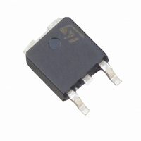
... N-channel 100V - 0.025Ω - 50A TO-220 / DPAK Low gate charge STripFET™ II Power MOSFET Max I DS(on) D <0.028Ω 50A <0.028Ω 50A Figure 1. Marking P40NF10 D40NF10 Rev 4 STD40NF10 STP40NF10 3 1 DPAK TO-220 Internal schematic diagram Package Packaging TO-220 Tube DPAK Tape & reel 3 2 ...
Page 2
... Contents Contents 1 Electrical ratings . . . . . . . . . . . . . . . . . . . . . . . . . . . . . . . . . . . . . . . . . . . . 3 2 Electrical characteristics . . . . . . . . . . . . . . . . . . . . . . . . . . . . . . . . . . . . . 4 2.1 Electrical characteristics (curves) 3 Test circuit 4 Package mechanical data . . . . . . . . . . . . . . . . . . . . . . . . . . . . . . . . . . . . 10 5 Packaging mechanical data . . . . . . . . . . . . . . . . . . . . . . . . . . . . . . . . . . 13 6 Revision history . . . . . . . . . . . . . . . . . . . . . . . . . . . . . . . . . . . . . . . . . . . 14 2/ STP40NF10 - STD40NF10 . . . . . . . . . . . . . . . . . . . . . . . . . . . . 6 ...
Page 3
... STP40NF10 - STD40NF10 1 Electrical ratings Table 2. Absolute maximum ratings Symbol V Drain-source voltage ( Gate- source voltage GS (1) I Drain current (continuous Drain current (continuous (2) I Drain current (pulsed Total dissipation at T TOT Derating factor (3) dv/dt Peak diode recovery voltage slope (4) E Single pulse avalanche energy ...
Page 4
... MHz 50V 10V GS (see Figure 17) Parameter Test conditions V = 50V 4.7Ω (see Figure 16 27V 4.7Ω (see Figure 16) STP40NF10 - STD40NF10 Min. Typ 100 GS =125° 250µ 25A 0.025 D Min. Typ. I =28A 22 D 2180 298 83.7 46.5 = 40A, D 13.3 17.5 Min ...
Page 5
... STP40NF10 - STD40NF10 Table 7. Source drain diode Symbol I Source-drain current SD (1) I Source-drain current (pulsed) SDM (2) V Forward on voltage SD t Reverse recovery time rr Q Reverse recovery charge rr I Reverse recovery current RRM 1. Pulse width limited by safe operating area. 2. Pulsed: Pulse duration = 300 µs, duty cycle 1.5% ...
Page 6
... Electrical characteristics 2.1 Electrical characteristics (curves) Figure 2. Safe operating area for TO-220 Figure 4. Safe operating area for DPAK Figure 6. Output characteristics 6/15 STP40NF10 - STD40NF10 Figure 3. Thermal impedance for TO-220 Figure 5. Thermal impedance for DPAK Figure 7. Transfer characteristics ...
Page 7
... STP40NF10 - STD40NF10 Figure 8. Transconductance Figure 10. Gate charge vs. gate-source voltage Figure 11. Capacitance variations Figure 12. Normalized gate threshold voltage vs. temperature Electrical characteristics Figure 9. Static drain-source on resistance Figure 13. Normalized on resistance vs. temperature 7/15 ...
Page 8
... Electrical characteristics Figure 14. Source-drain diode forward characteristics 8/15 STP40NF10 - STD40NF10 Figure 15. Normalized breakdown voltage vs. tj ...
Page 9
... STP40NF10 - STD40NF10 3 Test circuit Figure 16. Switching times test circuit for resistive load Figure 18. Test circuit for inductive load switching and diode recovery times Figure 20. Unclamped inductive waveform Figure 17. Gate charge test circuit Figure 19. Unclamped Inductive load test circuit Figure 21. Switching time waveform ...
Page 10
... These packages have a Lead-free second level interconnect . The category of second level interconnect is marked on the package and on the inner box label, in compliance with JEDEC Standard JESD97. The maximum ratings related to soldering conditions are also marked on the inner box label. ECOPACK trademark. ECOPACK specifications are available at : 10/15 STP40NF10 - STD40NF10 www.st.com ...
Page 11
... STP40NF10 - STD40NF10 Dim L20 L30 ∅P Q TO-220 mechanical data mm Min Typ Max 4.40 4.60 0.61 0.88 1.14 1.70 0.49 0.70 15.25 15.75 1.27 10 10.40 2.40 2.70 4.95 5.15 1.23 1.32 6.20 6.60 2.40 2. 3.50 3.93 16.40 28.90 3.75 3.85 2.65 2.95 ...
Page 12
... STP40NF10 - STD40NF10 inch MIN. TYP. MAX. 0.086 0.094 0.035 0.043 0.001 0.009 0.025 0.035 0.204 0.212 0.017 0.023 0.019 0.023 0.236 0.244 0.200 ...
Page 13
... STP40NF10 - STD40NF10 5 Packaging mechanical data DPAK FOOTPRINT All dimensions are in millimeters TAPE MECHANICAL DATA mm DIM. MIN. MAX 10.4 10.6 B1 12.1 D 1.5 1.6 D1 1.5 E 1.65 1.85 F 7.4 7.6 K0 2.55 2.75 P0 3.9 4.1 P1 7.9 8.1 P2 1.9 2 15.7 16.3 TAPE AND REEL SHIPMENT inch MIN ...
Page 14
... Revision history 6 Revision history Table 8. Document revision history Date 16-Dec-2004 17-Aug-2006 31-Jan-2007 19-Sep-2007 14/15 Revision 1 First version. 2 The document has been reformatted. 3 Typo mistake on Table 4 Added DPAK STP40NF10 - STD40NF10 Changes 2. ...
Page 15
... STP40NF10 - STD40NF10 Information in this document is provided solely in connection with ST products. STMicroelectronics NV and its subsidiaries (“ST”) reserve the right to make changes, corrections, modifications or improvements, to this document, and the products and services described herein at any time, without notice. All ST products are sold pursuant to ST’s terms and conditions of sale. ...