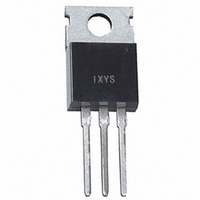
IXTP90N055T IXYS, IXTP90N055T Datasheet - Page 2

IXTP90N055T
Manufacturer Part Number
IXTP90N055T
Description
MOSFET N-CH 55V 90A TO-220
Manufacturer
IXYS
Series
TrenchT2™r
Datasheet
1.IXTP90N055T.pdf
(5 pages)
Specifications of IXTP90N055T
Fet Type
MOSFET N-Channel, Metal Oxide
Fet Feature
Standard
Rds On (max) @ Id, Vgs
8.8 mOhm @ 25A, 10V
Drain To Source Voltage (vdss)
55V
Current - Continuous Drain (id) @ 25° C
90A
Vgs(th) (max) @ Id
4V @ 50µA
Gate Charge (qg) @ Vgs
61nC @ 10V
Input Capacitance (ciss) @ Vds
2500pF @ 25V
Power - Max
176W
Mounting Type
Through Hole
Package / Case
TO-220
Configuration
Single
Transistor Polarity
N-Channel
Resistance Drain-source Rds (on)
0.0088 Ohms
Forward Transconductance Gfs (max / Min)
55 s
Drain-source Breakdown Voltage
55 V
Continuous Drain Current
90 A
Power Dissipation
176 W
Maximum Operating Temperature
+ 175 C
Mounting Style
Through Hole
Minimum Operating Temperature
- 55 C
Vdss, Max, (v)
55
Id(cont), Tc=25°c, (a)
90
Rds(on), Max, Tj=25°c, (?)
0.0088
Ciss, Typ, (pf)
2500
Qg, Typ, (nc)
61
Trr, Typ, (ns)
70
Trr, Max, (ns)
-
Pd, (w)
176
Rthjc, Max, (k/w)
0.85
Package Style
TO-220
Lead Free Status / RoHS Status
Lead free / RoHS Compliant
Symbol
(T
g
C
C
C
t
t
t
t
Q
Q
Q
R
R
Source-Drain Diode
Symbol
T
I
I
V
t
IXYS MOSFETs and IGBTs are covered by 4,835,592
SM
d(on)
d(off)
f
S
r
rr
Notes: 1.
one or moreof the following U.S. patents:
IXYS reserves the right to change limits, test conditions, and dimensions.
fs
J
oss
thJC
thCS
SD
iss
rss
g(on)
gs
gd
The product presented herein is under development. The Technical Specifications
offered are derived from data gathered during objective characterizations of preliminary
engineering lots; but also may yet contain some information supplied during a pre-
production design evaluation. IXYS reserves the right to change limits, test conditions,
and dimensions without notice.
J
= 25° C unless otherwise specified)
= 25° C unless otherwise specified)
2. On through-hole packages, R
location must be 5 mm or less from the package body.
Pulse test, t ≤ 300 µs, duty cycle d ≤ 2 %;
Test Conditions
V
V
Resistive Switching Times
V
R
V
TO-220
Test Conditions
V
Pulse width limited by T
I
I
V
F
F
DS
GS
GS
GS
GS
R
G
= 25 A, V
= 25 A, -di/dt = 100 A/µs
= 25 V, V
= 10 Ω (External)
= 10 V; I
= 10 V, V
PRELIMINARY TECHNICAL INFORMATION
= 0 V
= 0 V, V
= 10 V, V
GS
DS
D
GS
DS
DS
= 0.5 I
= 0 V, Note 1
= 25 V, f = 1 MHz
= 0 V
= 0.5 V
= 0.5 V
4,850,072
4,881,106
D25
, Note 1
DSS
DSS
JM
4,931,844
5,017,508
5,034,796
, I
, I
D
D
DS(on)
= 10 A
= 10 A
Kelvin test contact
5,049,961
5,063,307
5,187,117
Min.
Min.
5,237,481
5,381,025
5,486,715
30
Characteristic Values
Characteristic Values
2500
Typ.
Typ.
0.50
440
113
55
19
30
40
20
61
15
11
70
6,162,665
6,259,123 B1
6,306,728 B1
Max.
Max.
0.85 °C/W
240
1.0
90
°C/W
6,404,065 B1
6,534,343
6,583,505
nC
nC
nC
pF
pF
pF
n s
n s
n s
n s
n s
S
V
A
A
TO-263 (IXTA) Outline
TO-220 (IXTP) Outline
6,683,344
6,710,405B2
6,710,463
Pins: 1 - Gate
Dim.
A
A1
b
b2
c
c2
D
D1
E
E1
e
L
L1
L2
L3
L4
R
Pins: 1 - Gate
3 - Source 4, TAB - Drain
14.61
4.06
2.03
0.51
1.14
0.46
1.14
8.64
7.11
9.65
6.86
2.54
2.29
1.02
1.27
0.46
Min.
3 - Source 4, TAB - Drain
Millimeter
0
6,727,585
6,759,692
6771478 B2
IXTP90N055T
10.29
15.88
IXTA90N055T
Max.
BSC
4.83
2.79
0.99
1.40
0.74
1.40
9.65
8.13
8.13
2.79
1.40
1.78
0.38
0.74
2 - Drain
2 - Drain
.160
.080
.020
.045
.018
.045
.340
.280
.380
.270
.100
.575
.090
.040
.050
.018
Min.
7,005,734 B2
7,063,975 B2
7,071,537
Inches
0
Max.
BSC
.190
.110
.039
.055
.029
.055
.380
.320
.405
.320
.625
.110
.055
.070
.015
.029


