STD5NM50T4 STMicroelectronics, STD5NM50T4 Datasheet
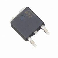
MOSFET N-CH 500V 7.5A DPAK

STD5NM50T4

Manufacturer Part Number
STD5NM50T4
Description
MOSFET N-CH 500V 7.5A DPAK
Manufacturer
STMicroelectronics
Series
MDmesh™r
Datasheet

Specifications of STD5NM50T4

Fet Type
MOSFET N-Channel, Metal Oxide
Fet Feature
Standard
Rds On (max) @ Id, Vgs
800 mOhm @ 2.5A, 10V
Drain To Source Voltage (vdss)
500V
Current - Continuous Drain (id) @ 25° C
7.5A
Vgs(th) (max) @ Id
5V @ 250µA
Gate Charge (qg) @ Vgs
13nC @ 10V
Input Capacitance (ciss) @ Vds
415pF @ 25V
Power - Max
100W
Mounting Type
Surface Mount
Package / Case
DPak, TO-252 (2 leads+tab), SC-63
Configuration
Single
Transistor Polarity
N-Channel
Resistance Drain-source Rds (on)
0.8 Ohms
Forward Transconductance Gfs (max / Min)
3.5 S
Drain-source Breakdown Voltage
500 V
Gate-source Breakdown Voltage
+/- 30 V
Continuous Drain Current
7.5 A
Power Dissipation
100 W
Maximum Operating Temperature
+ 150 C
Mounting Style
SMD/SMT
Minimum Operating Temperature
- 55 C
Lead Free Status / RoHS Status
Lead free / RoHS Compliant
Other names
497-3162-2

Available stocks

Company
Part Number
Manufacturer
Quantity
Price
Part Number:
STD5NM50T4
Manufacturer:
ST
0
Part Number:
STD5NM50T4G
Manufacturer:
ST
0
n
n
n
n
n
n
DESCRIPTION
The MDmesh™ is a new revolutionary MOSFET
technology that associates the Multiple Drain pro-
cess with the Company’s PowerMESH™ horizontal
layout. The resulting product has an outstanding low
on-resistance, impressively high dv/dt and excellent
avalanche characteristics. The adoption of the
Company’s proprietary strip technique yields overall
dynamic performance that is significantly better than
that of similar competition’s products.
APPLICATIONS
The MDmesh™ family is very suitable for increasing
power density of high voltage converters allowing
system miniaturization and higher efficiencies.
ABSOLUTE MAXIMUM RATINGS
(•)Pulse width limited by safe operating area
September 2002
STD5NM50
STD5NM50-1
TYPICAL R
HIGH dv/dt AND AVALANCHE CAPABILITIES
100% AVALANCHE TESTED
LOW INPUT CAPACITANCE AND GATE
CHARGE
LOW GATE INPUT RESISTANCE
TIGHT PROCESS CONTROL AND HIGH
MANUFACTURING YIELDS
dv/dt (1)
Symbol
I
V
DM
P
V
V
T
DGR
I
I
TOT
T
stg
DS
GS
D
D
TYPE
j
(
l
)
Drain-source Voltage (V
Drain-gate Voltage (R
Gate- source Voltage
Drain Current (continuous) at T
Drain Current (pulsed)
Total Dissipation at T
Derating Factor
Peak Diode Recovery voltage slope
Storage Temperature
Max. Operating Junction Temperature
DS
(on) = 0.7
500V
500V
V
DSS
R
N-CHANNEL 500V - 0.7 - 7.5A DPAK/IPAK
<0.8
<0.8
DS(on)
C
GS
Parameter
= 25°C
GS
= 20 k )
= 0)
C
C
7.5 A
7.5 A
= 25°C
= 100°C
I
D
(1) I
SD
MDmesh™Power MOSFET
INTERNAL SCHEMATIC DIAGRAM
5A, di/dt
TO-252
DPAK
1
400A/µs, V
3
– 55 to 150
STD5NM50-1
Value
DD
500
500
±30
100
7.5
4.7
0.8
30
15
STD5NM50
V
(Add Suffix “-1”)
(BR)DSS
TO-251
IPAK
, T
j
T
JMAX.
1
2
W/°C
V/ns
3
Unit
1/10
°C
W
V
V
V
A
A
A

Related parts for STD5NM50T4

STD5NM50T4 Summary of contents

Page 1

TYPE V DSS STD5NM50 500V STD5NM50-1 500V n TYPICAL R (on HIGH dv/dt AND AVALANCHE CAPABILITIES 100% AVALANCHE TESTED n LOW INPUT CAPACITANCE AND GATE n CHARGE n LOW GATE INPUT RESISTANCE TIGHT PROCESS CONTROL AND ...

Page 2

STD5NM50/STD5NM50-1 THERMAL DATA Rthj-case Thermal Resistance Junction-case Rthj-amb Thermal Resistance Junction-ambient T Maximum Lead Temperature For Soldering Purpose l AVALANCHE CHARACTERISTICS Symbol I Avalanche Current, Repetitive or Not-Repetitive AR (pulse width limited Single Pulse Avalanche Energy AS ...

Page 3

ELECTRICAL CHARACTERISTICS (CONTINUED) SWITCHING ON Symbol Parameter t Turn-on Delay Time d(on) t Rise Time r Q Total Gate Charge g Q Gate-Source Charge gs Q Gate-Drain Charge gd SWITCHING OFF Symbol Parameter t Off-voltage Rise Time r(Voff) t Fall ...

Page 4

STD5NM50/STD5NM50-1 Output Characteristics Transconductance Gate Charge vs Gate-source Voltage 4/10 Transfer Characteristics Static Drain-source On Resistance Capacitance Variations ...

Page 5

Normalized Gate Threshold Voltage vs Temperature Source-drain Diode Forward Characteristics STD5NM50/STD5NM50-1 Normalized On Resistance vs Temperature Normalized BVDSS vs Temperature 5/10 ...

Page 6

STD5NM50/STD5NM50-1 Fig. 1: Unclamped Inductive Load Test Circuit Fig. 3: Switching Times Test Circuit For Resistive Load Fig. 5: Test Circuit For Inductive Load Switching And Diode Recovery Times 6/10 Fig. 2: Unclamped Inductive Waveform Fig. 4: Gate Charge test ...

Page 7

TO-252 (DPAK) MECHANICAL DATA mm DIM. MIN. TYP. A 2.20 A1 0.90 A2 0.03 B 0.64 B2 5.20 C 0.45 C2 0.48 D 6.00 E 6.40 G 4.40 H 9.35 L2 0 STD5NM50/STD5NM50-1 inch MAX. ...

Page 8

STD5NM50/STD5NM50-1 DIM. MIN. A 2.2 A1 0.9 A3 0.7 B 0. 0. 6.4 G 4 0.8 L2 8/10 TO-251 (IPAK) MECHANICAL DATA mm TYP. ...

Page 9

STD5NM50/STD5NM50-1 DPAK FOOTPRINT All dimensions are in millimeters TAPE AND REEL SHIPMENT (suffix ”T4”)* TAPE MECHANICAL DATA mm DIM. MIN. MAX. MIN. A0 6.8 7 0.267 0.275 B0 10.4 10.6 0.409 0.417 B1 12.1 D 1.5 1.6 0.059 0.063 D1 ...

Page 10

... No license is granted by implication or otherwise under any patent or patent rights of STMicroelectronics. Specifications mentioned in this publication are subject to change without notice. This publication supersedes and replaces all information previously supplied ...

Related keywords