STW120NF10 STMicroelectronics, STW120NF10 Datasheet

MOSFET N-CH 100V 110A TO-247

STW120NF10

Manufacturer Part Number
STW120NF10
Description
MOSFET N-CH 100V 110A TO-247
Manufacturer
STMicroelectronics
Series
STripFET™r
Datasheets

Specifications of STW120NF10

Fet Type
MOSFET N-Channel, Metal Oxide
Fet Feature
Standard
Rds On (max) @ Id, Vgs
10.5 mOhm @ 60A, 10V
Drain To Source Voltage (vdss)
100V
Current - Continuous Drain (id) @ 25° C
110A
Vgs(th) (max) @ Id
4V @ 250µA
Gate Charge (qg) @ Vgs
233nC @ 10V
Input Capacitance (ciss) @ Vds
5200pF @ 25V
Power - Max
312W
Mounting Type
Through Hole
Package / Case
TO-247-3
Configuration
Single
Transistor Polarity
N-Channel
Resistance Drain-source Rds (on)
0.009 Ohms
Drain-source Breakdown Voltage
100 V
Gate-source Breakdown Voltage
+/- 20 V
Continuous Drain Current
110 A
Power Dissipation
312 W
Maximum Operating Temperature
+ 175 C
Mounting Style
Through Hole
Minimum Operating Temperature
- 55 C
Current, Drain
110 A
Gate Charge, Total
172 nC
Package Type
TO-247
Polarization
N-Channel
Resistance, Drain To Source On
0.009 Ohm
Temperature, Operating, Maximum
+175 °C
Temperature, Operating, Minimum
-55 °C
Time, Turn-off Delay
132 ns
Time, Turn-on Delay
25 ns
Transconductance, Forward
90 S
Voltage, Breakdown, Drain To Source
100 V
Voltage, Forward, Diode
1.3 V
Voltage, Gate To Source
±20 V
Continuous Drain Current Id
60A
Drain Source Voltage Vds
100V
On Resistance Rds(on)
9mohm
Rds(on) Test Voltage Vgs
10V
Threshold Voltage Vgs Typ
4V
Rohs Compliant
Yes
Lead Free Status / RoHS Status
Lead free / RoHS Compliant
Other names
497-5166-5

Available stocks

Company
Part Number
Manufacturer
Quantity
Price
Part Number:
STW120NF10
Manufacturer:
ST
0
General features
Description
This Power MOSFET series realized with
STMicroelectronics unique STripFET™ process
has specifically been designed to minimize the
on-resistance. It is therefore suitable as primary
switch in advanced high-efficiency,high-frequency
isolated DC-DC converters for Telecom and
Computer application. It is also intended for any
applications with low gate drive requirements.
Applications
Order codes
STW120NF10
STP120NF10
STB120NF10
Exceptional dv/dt capability
100% avalanche tested
Application oriented characterization
Switching application
Type
STW120NF10
STP120NF10
STB120NF10
Part number
N-channel 100V - 0.009Ω - 110A - TO-247 - TO-220 - D²PAK
V
100V
100V
100V
DSS
<0.0105Ω
<0.0105Ω
<0.0105Ω
R
DS(on)
W120NF10
P120NF10
B120NF10
Marking
110A
110A
110A
I
D
STP120NF10 - STB120NF10
Internal schematic diagram
STripFET™ II Power MOSFET
D²PAK
Package
TO-247
TO-220
D²PAK
1
3
TO-220
STW120NF10
1
2
3
Packaging
Tape & reel
TO-247
Tube
Tube
1/15
15

Related parts for STW120NF10

STW120NF10 Summary of contents

Page 1

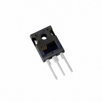
... STB120NF10 STP120NF10 - STB120NF10 STripFET™ II Power MOSFET R I DS(on) D <0.0105Ω 110A <0.0105Ω 110A <0.0105Ω 110A Internal schematic diagram Marking W120NF10 P120NF10 B120NF10 STW120NF10 3 1 TO-247 D²PAK TO-220 Package Packaging TO-247 Tube TO-220 Tube D²PAK Tape & reel 1/15 ...

Page 2

... STW120NF10 - STP120NF10 - STB120NF10 1 Electrical ratings Table 1. Absolute maximum ratings Symbol V Drain-source voltage ( Gate-source voltage GS I Drain current (continuous Drain current (continuous (1) I Drain current (pulsed Total dissipation at T TOT Derating factor (2) dv/dt Peak diode recovery voltage slope (3) E Single pulse avalanche energy ...

Page 3

... C Input capacitance iss Output capacitance C oss Reverse transfer C rss capacitance Q Total gate charge g Q Gate-source charge gs Gate-drain charge Pulsed: pulse duration=300µs, duty cycle 1.5% 4/15 STW120NF10 - STP120NF10 - STB120NF10 Parameter Test conditions I = 250µ Max rating Max rating@125° ±20V ...

Page 4

... STW120NF10 - STP120NF10 - STB120NF10 Table 5. Switching times Symbol t d(on) Turn-on delay time t Rise time r t Turn-off delay time d(off) Fall time t f Table 6. Source drain diode Symbol I Source-drain current SD (1) I Source-drain current (pulsed) SDM (2) V Forward on voltage SD t Reverse recovery time rr Q Reverse recovery charge ...

Page 5

... STW120NF10 - STP120NF10 - STB120NF10 4 Package mechanical data In order to meet environmental requirements, ST offers these devices in ECOPACK® packages. These packages have a Lead-free second level interconnect . The category of second level interconnect is marked on the package and on the inner box label, in compliance with JEDEC Standard JESD97. The maximum ratings related to soldering conditions are also marked on the inner box label ...

Page 6

... Package mechanical data DIM øP øR S 10/15 STW120NF10 - STP120NF10 - STB120NF10 TO-247 MECHANICAL DATA mm. MIN. TYP MAX. 4.85 5.15 2.20 2.60 1.0 1.40 2.0 2.40 3.0 3.40 0.40 0.80 19.85 20.15 15.45 15.75 5.45 14.20 14.80 3.70 4.30 18.50 3.55 3.65 4.50 5 ...

Related keywords