IXFV12N90PS IXYS, IXFV12N90PS Datasheet - Page 2
IXFV12N90PS
Manufacturer Part Number
IXFV12N90PS
Description
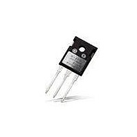
MOSFET N-CH 900V 12A PLUS220SMD
Manufacturer
IXYS
Series
Polar™r
Type
Polar Power MOSFETr
Datasheet
1.IXFH12N90P.pdf
(4 pages)
Specifications of IXFV12N90PS
Fet Type
MOSFET N-Channel, Metal Oxide
Fet Feature
Standard
Rds On (max) @ Id, Vgs
900 mOhm @ 500mA, 10V
Drain To Source Voltage (vdss)
900V
Current - Continuous Drain (id) @ 25° C
12A
Vgs(th) (max) @ Id
6.5V @ 1mA
Gate Charge (qg) @ Vgs
56nC @ 10V
Input Capacitance (ciss) @ Vds
3080pF @ 25V
Power - Max
380W
Mounting Type
Surface Mount
Package / Case
PLUS-220SMD
Product
MOSFET Gate Drivers
Rise Time
32 ns
Fall Time
68 ns
Supply Current
12 A
Maximum Power Dissipation
380 W
Maximum Operating Temperature
+ 150 C
Mounting Style
Through Hole
Maximum Turn-off Delay Time
50 ns
Maximum Turn-on Delay Time
32 ns
Minimum Operating Temperature
- 55 C
Number Of Drivers
Single
Number Of Outputs
1
Output Current
12 A
Output Voltage
900 V
Vdss, Max, (v)
900
Id(cont), Tc=25°c, (a)
12
Rds(on), Max, Tj=25°c, (?)
0.90
Ciss, Typ, (pf)
3080
Qg, Typ, (nc)
56
Trr, Typ, (ns)
-
Trr, Max, (ns)
300
Pd, (w)
380
Rthjc, Max, (ºc/w)
0.33
Package Style
PLUS220SMD
Lead Free Status / RoHS Status
Lead free / RoHS Compliant


Symbol
(T
g
R
C
C
C
t
t
t
t
Q
Q
Q
R
R
Source-Drain Diode
T
I
I
V
t
Q
I
Note 1: Pulse test, t ≤ 300μs; duty cycle, d ≤ 2%.
IXYS reserves the right to change limits, test conditions, and dimensions.
IXYS MOSFETs and IGBTs are covered
by one or more of the following U.S. patents: 4,850,072
S
SM
RM
d(on)
r
d(off)
f
rr
fs
J
PLUS220SMD (IXFV_S) Outline
SD
Gi
iss
oss
rss
thJC
thCS
The product presented herein is under development. The Technical Specifications offered are derived
from data gathered during objective characterizations of preliminary engineering lots; but also may yet
contain some information supplied during a pre-production design evaluation. IXYS reserves the right
to change limits, test conditions, and dimensions without notice.
g(on)
gs
gd
RM
J
= 25°C unless otherwise specified)
= 25°C unless otherwise specified)
Resistive Switching Times
V
R
I
V
Test Conditions
V
Gate input resistance
V
V
(TO-247, PLUS220)
V
Repetitive, pulse width limited by T
I
F
F
GS
R
DS
GS
G
GS
GS
= 6A, -di/dt = 100A/μs
= I
= 100V, V
PRELIMINARY TECHNICAL INFORMATION
= 10V, V
= 2Ω (External)
= 0V
= 20V, I
= 10V, V
S
= 0V, V
, V
GS
= 0V, Note 1
D
DS
DS
GS
DS
= 0.5 • I
= 0.5 • V
= 25V, f = 1MHz
= 0V
4,835,592
4,881,106
= 0.5 • V
D25
DSS
, Note 1
4,931,844
5,017,508
5,034,796
DSS
, I
, I
D
D
= 0.5 • I
= 0.5 • I
5,049,961
5,063,307
5,187,117
JM
D25
D25
5,237,481
5,381,025
5,486,715
Min.
5.0
Min.
Characteristic Values
Characteristic Values
6,162,665
6,259,123 B1
6,306,728 B1
Typ.
3080
Typ.
0.25
200
0.9
7.8
8.2
1.7
33
32
56
18
27
34
50
68
0.33 °C/W
6,404,065 B1
6,534,343
6,583,505
Max.
Max.
300 ns
1.5
12
48
°C/W
nC
nC
nC
μC
pF
pF
pF
ns
ns
ns
ns
Ω
S
A
A
V
A
IXFH12N90P IXFV12N90P
6,683,344
6,710,405 B2 6,759,692
6,710,463
TO-247 (IXFH) Outline
PLUS220 (IXFV) Outline
Dim.
A
A
A
b
b
b
C
D
E
e
L
L1
∅P
Q
R
S
6,727,585
1
2
6,771,478 B2 7,071,537
1
2
20.80
15.75
19.81
1.65
2.87
5.20
3.55
5.89
4.32
6.15
Min.
4.7
2.2
2.2
1.0
Millimeter
.4
21.46
16.26
20.32
BSC
7,005,734 B2
7,063,975 B2
Max.
IXFV12N90PS
2.54
2.13
3.12
5.72
4.50
3.65
6.40
5.49
5.3
2.6
1.4
e
.8
∅ P
0.205 0.225
0.232 0.252
.185
.087
.059
.040
.065
.113
.016
.819
.610
.780
.140
.170
Min.
242
Inches
7,157,338B2
Max.
BSC
.209
.102
.098
.055
.084
.123
.031
.845
.640
.800
.177
.144
.216
Related parts for IXFV12N90PS
Image
Part Number
Description
Manufacturer
Datasheet
Request
R


Part Number:
Description:
HiPerFET Power MOSFETs
Manufacturer:
IXYS Corporation
Datasheet:
Part Number:
Description:
J-K-Type Flip-Flop
Manufacturer:
IXYS Corporation
Datasheet:
Part Number:
Description:
HiPerRF Power MOSFETs
Manufacturer:
IXYS Corporation
Datasheet:
Part Number:
Description:
Rectifier Module for Three Phase Power Factor Correction
Manufacturer:
IXYS Corporation
Datasheet:
Part Number:
Description:
Thyristor Modules Thyristor/Diode Modules
Manufacturer:
IXYS Corporation
Datasheet:
Part Number:
Description:
Thyristor Modules Thyristor/Diode Modules
Manufacturer:
IXYS Corporation
Datasheet:
Part Number:
Description:
Thyristor Modules Thyristor/Diode Modules
Manufacturer:
IXYS Corporation
Datasheet:
Part Number:
Description:
Thyristor Modules Thyristor/Diode Modules
Manufacturer:
IXYS Corporation
Datasheet:
Part Number:
Description:
Thyristor Modules /Diode Modules
Manufacturer:
IXYS Corporation
Datasheet:
Part Number:
Description:
Thyristor Modules /Diode Modules
Manufacturer:
IXYS Corporation
Datasheet:
Part Number:
Description:
Thyristor Modules Thyristor/Diode Modules
Manufacturer:
IXYS Corporation
Datasheet: