STD11NM60N STMicroelectronics, STD11NM60N Datasheet - Page 4
STD11NM60N
Manufacturer Part Number
STD11NM60N
Description
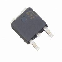
MOSFET N-CH 600V 10A DPAK
Manufacturer
STMicroelectronics
Series
MDmesh™r
Datasheet
1.STD11NM60N-1.pdf
(20 pages)
Specifications of STD11NM60N
Fet Type
MOSFET N-Channel, Metal Oxide
Fet Feature
Standard
Rds On (max) @ Id, Vgs
450 mOhm @ 5A, 10V
Drain To Source Voltage (vdss)
600V
Current - Continuous Drain (id) @ 25° C
10A
Vgs(th) (max) @ Id
4V @ 250µA
Gate Charge (qg) @ Vgs
31nC @ 10V
Input Capacitance (ciss) @ Vds
850pF @ 50V
Power - Max
90W
Mounting Type
Surface Mount
Package / Case
DPak, TO-252 (2 leads+tab), SC-63
Lead Free Status / RoHS Status
Lead free / RoHS Compliant
Other names
497-5733-2
Available stocks
Company
Part Number
Manufacturer
Quantity
Price
Company:

Part Number:
STD11NM60N
Manufacturer:
ST
Quantity:
12 500
Company:
Part Number:
STD11NM60N-1
Manufacturer:
ST
Quantity:
12 500


Electrical characteristics
2
4/20
Electrical characteristics
(T
Table 5.
1.
Table 6.
1.
2. C
C
V
Symbol
Symbol
R
dv/dt
CASE
V
oss eq.
(BR)DSS
g
C
I
I
increases from 0 to 80% V
DS(on)
C
C
GS(th)
Q
Q
Characteristic value at turn off on inductive load
Pulsed: pulse duration = 300µs, duty cycle 1.5%
DSS
GSS
Rg
Q
fs
oss
oss eq.
rss
iss
gs
gd
(1)
g
(1)
=25 °C unless otherwise specified)
(2)
is defined as a constant equivalent capacitance giving the same charging time as C
Forward transconductance
Input capacitance
Output capacitance
Reverse transfer
capacitance
Equivalent output
capacitance
Gate input resistance
Total gate charge
Gate-source charge
Gate-drain charge
Drain-source breakdown
voltage
Drain-source voltage slope
Zero gate voltage drain
current (V
Gate body leakage current
(V
Gate threshold voltage
Static drain-source on
resistance
On/off states
Dynamic
DS
= 0)
Parameter
Parameter
GS
= 0)
DSS
V
V
V
V
f=1 MHz Gate DC Bias=0
Test signal level=20 mV
open drain
V
V
Figure 19
I
V
V
V
V
V
V
V
D
GS
GS
GS
DS
DS
DD
DD
GS
DS
DS
GS
DS
GS
= 1 mA, V
=0
=0, V
=480 V, I
=Max rating,Tc=125 °C
= V
= 10 V, I
=15 V, I
=50 V, f=1 MHz,
=10 V
= Max rating,
= ±20 V
= 400 V,I
=10 V
Test conditions
Test conditions
GS
DS
, I
D
=0 to 480 V
D
GS
D
D
D
= 5 A
= 250 µA
= 5 A
= 10 A
= 0
= 5 A,
Min.
Min.
600
2
Typ.
15.9
850
130
Typ.
0.37
7.5
3.7
4.2
44
31
5
45
3
oss
STx11NM60N
Max.
Max.
±
when V
0.45
100
10
1
4
DS
Unit
V/ns
Unit
nC
nC
nC
pF
pF
pF
pF
µA
µA
nA
Ω
S
Ω
V
V
Related parts for STD11NM60N
Image
Part Number
Description
Manufacturer
Datasheet
Request
R

Part Number:
Description:
STMicroelectronics [RIPPLE-CARRY BINARY COUNTER/DIVIDERS]
Manufacturer:
STMicroelectronics
Datasheet:
Part Number:
Description:
STMicroelectronics [LIQUID-CRYSTAL DISPLAY DRIVERS]
Manufacturer:
STMicroelectronics
Datasheet:

Part Number:
Description:
BOARD EVAL FOR MEMS SENSORS
Manufacturer:
STMicroelectronics
Datasheet:
Part Number:
Description:
NPN TRANSISTOR POWER MODULE
Manufacturer:
STMicroelectronics
Datasheet:
Part Number:
Description:
TURBOSWITCH ULTRA-FAST HIGH VOLTAGE DIODE
Manufacturer:
STMicroelectronics
Datasheet:
Part Number:
Description:
Manufacturer:
STMicroelectronics
Datasheet:
Part Number:
Description:
DIODE / SCR MODULE
Manufacturer:
STMicroelectronics
Datasheet:
Part Number:
Description:
DIODE / SCR MODULE
Manufacturer:
STMicroelectronics
Datasheet:
Part Number:
Description:
Search -----> STE16N100
Manufacturer:
STMicroelectronics
Datasheet:
Part Number:
Description:
Search ---> STE53NA50
Manufacturer:
STMicroelectronics
Datasheet:
Part Number:
Description:
NPN Transistor Power Module
Manufacturer:
STMicroelectronics
Datasheet:
Part Number:
Description:
DIODE / SCR MODULE
Manufacturer:
STMicroelectronics
Datasheet: