MTD2955VT4 ON Semiconductor, MTD2955VT4 Datasheet - Page 2
MTD2955VT4
Manufacturer Part Number
MTD2955VT4
Description
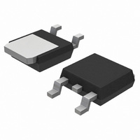
MOSFET P-CH 60V 12A DPAK
Manufacturer
ON Semiconductor
Datasheet
1.MTD2955VT4.pdf
(9 pages)
Specifications of MTD2955VT4
Fet Type
MOSFET P-Channel, Metal Oxide
Fet Feature
Standard
Rds On (max) @ Id, Vgs
230 mOhm @ 6A, 10V
Drain To Source Voltage (vdss)
60V
Current - Continuous Drain (id) @ 25° C
12A
Vgs(th) (max) @ Id
4V @ 250µA
Gate Charge (qg) @ Vgs
30nC @ 10V
Input Capacitance (ciss) @ Vds
770pF @ 25V
Power - Max
60W
Mounting Type
Surface Mount
Package / Case
DPak, TO-252 (2 leads+tab), SC-63
Lead Free Status / RoHS Status
Contains lead / RoHS non-compliant
Other names
MTD2955VT4OS
Available stocks
Company
Part Number
Manufacturer
Quantity
Price
Company:

Part Number:
MTD2955VT4
Manufacturer:
ONSEMI
Quantity:
905


3. Pulse Test: Pulse Width ≤ 300 ms, Duty Cycle ≤ 2%.
4. Switching characteristics are independent of operating junction temperature.
5. Reflects typical values.
OFF CHARACTERISTICS
ON CHARACTERISTICS (Note 3)
DYNAMIC CHARACTERISTICS
SWITCHING CHARACTERISTICS (Note 4)
SOURCE−DRAIN DIODE CHARACTERISTICS
INTERNAL PACKAGE INDUCTANCE
ELECTRICAL CHARACTERISTICS
Drain−to−Source Breakdown Voltage
Zero Gate Voltage Drain Current
Gate−Body Leakage Current (V
Gate Threshold Voltage
Static Drain−to−Source On−Resistance
Drain−to−Source On−Voltage
Forward Transconductance (V
Input Capacitance
Output Capacitance
Reverse Transfer Capacitance
Turn−On Delay Time
Rise Time
Turn−Off Delay Time
Fall Time
Gate Charge
Forward On−Voltage (Note 3)
Reverse Recovery Time
Reverse Recovery Stored
Internal Drain Inductance
Internal Source Inductance
(V
Temperature Coefficient (Positive)
(V
(V
(V
Threshold Temperature Coefficient (Negative)
(V
(V
(V
Charge
(Measured from contact screw on tab to center of die)
(Measured from the drain lead 0.25″ from package to center of die)
(Measured from the source lead 0.25″ from package to source bond pad)
GS
DS
DS
DS
GS
GS
GS
= 0 Vdc, I
= 60 Vdc, V
= 60 Vdc, V
= V
= 10 Vdc, I
= 10 Vdc, I
= 10 Vdc, I
GS
, I
D
D
= 250 mAdc)
D
D
D
= 0.25 mAdc)
GS
GS
= 6.0 Adc)
= 12 Adc)
= 6.0 Adc, T
= 0 Vdc)
= 0 Vdc, T
C
pk
=
Characteristic
DS
GS
J
J
= 10 Vdc, I
Max limit − Typ
= 150°C)
= 150°C)
= ± 20 Vdc, V
(I
3 x SIGMA
S
= 12 Adc, V
(T
(V
(V
(V
(I
(I
J
DS
S
S
DD
DS
D
= 25°C unless otherwise noted)
= 12 Adc, V
= 12 Adc, V
= 6.0 Adc)
= 25 Vdc, V
dI
= 30 Vdc, I
= 48 Vdc, I
DS
V
V
S
f = 1.0 MHz)
R
/dt = 100 A/ms)
GS
GS
GS
G
= 0 Vdc)
= 10 Vdc)
= 10 Vdc,
= 9.1 W)
= 0 Vdc, T
(Cpk ≥ 2.0) (Note 5)
(Cpk ≥ 2.0) (Note 5)
(Cpk ≥ 1.5) (Note 5)
http://onsemi.com
GS
GS
D
D
GS
= 12 Adc,
= 12 Adc,
= 0 Vdc)
= 0 Vdc,
= 0 Vdc,
J
= 150°C)
2
V
Symbol
R
V
V
(BR)DSS
t
t
I
I
C
Q
DS(on)
DS(on)
C
V
GS(th)
C
g
d(on)
d(off)
DSS
GSS
Q
Q
Q
Q
L
L
t
t
t
FS
oss
t
t
SD
rss
RR
iss
rr
a
b
D
r
f
S
T
1
2
3
Min
2.0
3.0
60
−
−
−
−
−
−
−
−
−
−
−
−
−
−
−
−
−
−
−
−
−
−
−
−
−
−
−
−
0.185
0.53
Typ
550
200
115
2.8
5.0
5.0
4.0
9.0
7.0
1.8
1.5
3.5
4.5
7.5
58
50
15
50
24
39
19
90
25
−
−
−
−
−
−
0.230
Max
100
100
770
280
100
100
4.0
2.9
2.5
3.0
10
30
50
80
30
−
−
−
−
−
−
−
−
−
−
−
−
−
−
−
mV/°C
mV/°C
mhos
mAdc
nAdc
Unit
Vdc
Vdc
Vdc
Vdc
nC
mC
nH
nH
pF
ns
ns
W
Related parts for MTD2955VT4
Image
Part Number
Description
Manufacturer
Datasheet
Request
R

Part Number:
Description:
ON Semiconductor [VOLTAGE REGULATOR]
Manufacturer:
ON Semiconductor
Datasheet:
Part Number:
Description:
357-036-542-201 CARDEDGE 36POS DL .156 BLK LOPRO
Manufacturer:
ON Semiconductor
Datasheet:
Part Number:
Description:
357-036-542-201 CARDEDGE 36POS DL .156 BLK LOPRO
Manufacturer:
ON Semiconductor
Datasheet:
Part Number:
Description:
357-036-542-201 CARDEDGE 36POS DL .156 BLK LOPRO
Manufacturer:
ON Semiconductor
Datasheet:
Part Number:
Description:
357-036-542-201 CARDEDGE 36POS DL .156 BLK LOPRO
Manufacturer:
ON Semiconductor
Datasheet:
Part Number:
Description:
357-036-542-201 CARDEDGE 36POS DL .156 BLK LOPRO
Manufacturer:
ON Semiconductor
Datasheet:
Part Number:
Description:
357-036-542-201 CARDEDGE 36POS DL .156 BLK LOPRO
Manufacturer:
ON Semiconductor
Datasheet:
Part Number:
Description:
357-036-542-201 CARDEDGE 36POS DL .156 BLK LOPRO
Manufacturer:
ON Semiconductor
Datasheet:
Part Number:
Description:
357-036-542-201 CARDEDGE 36POS DL .156 BLK LOPRO
Manufacturer:
ON Semiconductor
Datasheet:
Part Number:
Description:
357-036-542-201 CARDEDGE 36POS DL .156 BLK LOPRO
Manufacturer:
ON Semiconductor
Datasheet:
Part Number:
Description:
357-036-542-201 CARDEDGE 36POS DL .156 BLK LOPRO
Manufacturer:
ON Semiconductor
Datasheet:
Part Number:
Description:
Manufacturer:
ON Semiconductor
Datasheet:
Part Number:
Description:
Manufacturer:
ON Semiconductor
Datasheet: