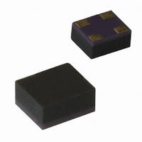
HMPP-389T-TR1 Avago Technologies US Inc., HMPP-389T-TR1 Datasheet - Page 10

HMPP-389T-TR1
Manufacturer Part Number
HMPP-389T-TR1
Description
DIODE PIN SWITCH 100V 1A MINIPAK
Manufacturer
Avago Technologies US Inc.
Datasheet
1.HMPP-3890-TR1.pdf
(13 pages)
Specifications of HMPP-389T-TR1
Package / Case
4-MiniPak (1412)
Diode Type
PIN - Single
Voltage - Peak Reverse (max)
100V
Current - Max
1A
Capacitance @ Vr, F
0.3pF @ 5V, 1MHz
Resistance @ If, F
2.5 Ohm @ 5mA, 100MHz
Configuration
Single Dual Common Anode Dual Common Cathode
Reverse Voltage
100 V
Forward Continuous Current
1 A
Frequency Range
SHF
Termination Style
SMD/SMT
Carrier Life
0.2 us
Maximum Diode Capacitance
0.3 pF @ 5 V
Maximum Operating Temperature
+ 150 C
Maximum Series Resistance @ Maximum If
2.5 Ohm @ 5 mA
Maximum Series Resistance @ Minimum If
3.8 Ohm (Typ) @ 1 mA
Minimum Operating Temperature
- 65 C
Mounting Style
SMD/SMT
Lead Free Status / RoHS Status
Contains lead / RoHS non-compliant
Power Dissipation (max)
-
Lead Free Status / Rohs Status
Lead free / RoHS Compliant
Available stocks
Company
Part Number
Manufacturer
Quantity
Price
Company:
Part Number:
HMPP-389T-TR1
Manufacturer:
AVAGO
Quantity:
9 000
Part Number:
HMPP-389T-TR1
Manufacturer:
AVAGO/安华高
Quantity:
20 000
Assembly Information
The MiniPak diode is mounted to the PCB or microstrip
board using the pad pattern shown in Figure 26.
Figure 6. PCB Pad Layout, MiniPak (dimensions in mm).
This mounting pad pattern is satisfactory for most
applications. However, there are applications where a
high degree of isolation is required between one diode
and the other is required. For such applications, the
mounting pad pattern of Figure 27 is recommended.
Figure 7. PCB Pad Layout, High Isolation MiniPak (dimensions in mm).
This pattern uses four via holes, connecting the crossed
ground strip pattern to the ground plane of the board.
10
0.40 mm via hole
(4 places)
0.8
0.40
0.4
0.5
2.60
0.4
0.20
0.3
0.5
0.3
2.40
SMT Assembly
Reliable assembly of surface mount components is a com-
plex process that involves many material, process, and
equipment factors, including: method of heating (e.g., IR
or vapor phase reflow, wave soldering, etc.) circuit board
material, conductor thickness and pattern, type of solder
alloy, and the thermal conductivity and thermal mass of
components. Components with a low mass, such as the
MiniPak package, will reach solder reflow temperatures
faster than those with a greater mass.
After ramping up from room temperature, the circuit
board with components attached to it (held in place with
solder paste) passes through one or more preheat zones.
The preheat zones increase the temperature of the board
and components to prevent thermal shock and begin
evaporating solvents from the solder paste. The reflow
zone briefly elevates the temperature sufficiently to pro-
duce a reflow of the solder.
The rates of change of temperature for the ramp-up and
cool-down zones are chosen to be low enough to not
cause deformation of the board or damage to compo-
nents due to thermal shock. The maximum temperature
in the reflow zone (T
These parameters are typical for a surface mount assembly
process for Avago diodes. As a general guideline, the
circuit board and components should be exposed only
to the minimum temperatures and times necessary to
achieve a uniform reflow of solder.
MAX
) should not exceed 260°C.


