HMPP-389T-TR1 Avago Technologies US Inc., HMPP-389T-TR1 Datasheet - Page 8
HMPP-389T-TR1
Manufacturer Part Number
HMPP-389T-TR1
Description
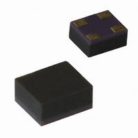
DIODE PIN SWITCH 100V 1A MINIPAK
Manufacturer
Avago Technologies US Inc.
Datasheet
1.HMPP-3890-TR1.pdf
(13 pages)
Specifications of HMPP-389T-TR1
Package / Case
4-MiniPak (1412)
Diode Type
PIN - Single
Voltage - Peak Reverse (max)
100V
Current - Max
1A
Capacitance @ Vr, F
0.3pF @ 5V, 1MHz
Resistance @ If, F
2.5 Ohm @ 5mA, 100MHz
Configuration
Single Dual Common Anode Dual Common Cathode
Reverse Voltage
100 V
Forward Continuous Current
1 A
Frequency Range
SHF
Termination Style
SMD/SMT
Carrier Life
0.2 us
Maximum Diode Capacitance
0.3 pF @ 5 V
Maximum Operating Temperature
+ 150 C
Maximum Series Resistance @ Maximum If
2.5 Ohm @ 5 mA
Maximum Series Resistance @ Minimum If
3.8 Ohm (Typ) @ 1 mA
Minimum Operating Temperature
- 65 C
Mounting Style
SMD/SMT
Lead Free Status / RoHS Status
Contains lead / RoHS non-compliant
Power Dissipation (max)
-
Lead Free Status / Rohs Status
Lead free / RoHS Compliant
Available stocks
Company
Part Number
Manufacturer
Quantity
Price
Company:

Part Number:
HMPP-389T-TR1
Manufacturer:
AVAGO
Quantity:
9 000
Part Number:
HMPP-389T-TR1
Manufacturer:
AVAGO/安华高
Quantity:
20 000


Testing the HMPP-389T on the Demo-board
Introduction
The HMPP-389T PIN diode is a high frequency shunt switch.
It has been designed as a smaller and higher performance
version of the HSMP-389T (SC-70 package).
The DEMO-HMPP-389T demo-board allows customers
to evaluate the performance of the HMPP-389T without
having to fabricate their own PCB. Since a shunt switch’s
isolation is limited primarily by its parasitic inductance, the
product’s true potential cannot be shown if a conventional
microstrip pcb is used. In order to overcome this problem,
a coplanar waveguide over ground-plane structure is
used for the demo-board. The bottom ground-plane is
connected to the upper ground traces using multiple
via-holes.
A 50Ω reference line is provided at the top to calibrate the
board loss. The bottom line allows the HMPP-389T diode
to be tested as a shunt switch.
Figure 17. Demo-board DEMO-HMPP-389T.
Demo-board Preparation
Since the performance of the shunt switch is ultimately
limited by the demo-board, a short discussion of the
constructional aspects will be beneficial. Edge-mounted
SMA connectors (Johnson #142-0701-881) were mounted
on both the reference and test lines. A special mounting
technique has been used to minimize reflection at the pcb
to connector interface. Prior to mounting, the connector
pins were cut down to two pin diameters in length. Subse-
quently, the connector fingers were soldered to the upper
ground plane (Figure 18). Solder was filled between the
connector body and fingers on the lower ground plane
until the small crescent of exposed teflon was completely
covered (Figure 19).
8
test line
reference line
HMPP-389T
SK063A
Agilent
Figure 18. Soldering details of connector fingers to upper ground plane.
Figure 19. Soldering details of connector fingers to lower ground plane.
Test Results
Measurements of the reference line’s return and insertion
losses were used to gauge the effectiveness of the VSWR
mitigating steps. In our prototype, the worst case return
loss of the reference line was 20 dB at 5 GHz (Figure 20).
Figure 0. Swept return loss of reference line.
Figure 15. Swept Return Loss of Reference
Line.
-18
-22
-26
-30
-34
-38
1
2
FREQUENCY (GHz)
3
4
5
6
Related parts for HMPP-389T-TR1
Image
Part Number
Description
Manufacturer
Datasheet
Request
R

Part Number:
Description:
DIODE PIN GP 50V 1A MINIPAK
Manufacturer:
Avago Technologies US Inc.
Datasheet:
Part Number:
Description:
DIODE PIN SWITCH 100V 1A MINIPAK
Manufacturer:
Avago Technologies US Inc.
Datasheet:

Part Number:
Description:
DIODE PIN RF SGL 50V 1A MINIPAK
Manufacturer:
Avago Technologies US Inc.
Datasheet:
Part Number:
Description:
DIODE PIN SGL 100V 1A MINIPAK
Manufacturer:
Avago Technologies US Inc.
Datasheet:

Part Number:
Description:
DIODE PIN RF SGL 50V 1A MINIPAK
Manufacturer:
Avago Technologies US Inc.
Datasheet:

Part Number:
Description:
DIODE PIN SGL 100V 1A MINIPAK
Manufacturer:
Avago Technologies US Inc.
Datasheet:
Part Number:
Description:
DIODE PIN SHUNT 100V 1A MINIPAK
Manufacturer:
Avago Technologies US Inc.
Datasheet:
Part Number:
Description:
DIODE PIN SHUNT 100V 1A MINIPAK
Manufacturer:
Avago Technologies US Inc.
Datasheet:
Part Number:
Description:
DIODE PIN GP 50V 1A MINIPAK
Manufacturer:
Avago Technologies US Inc.
Datasheet:
Part Number:
Description:
DIODE PIN GP 50V 1A MINIPAK
Manufacturer:
Avago Technologies US Inc.
Datasheet:

Part Number:
Description:
OPTOCOUPLER GATE DRV 2A 16-SOIC
Manufacturer:
Avago Technologies US Inc.
Datasheet:
Part Number:
Description:
OPTOCOUPLER 2CH 2.5A 16-SOIC
Manufacturer:
Avago Technologies US Inc.
Datasheet:

Part Number:
Description:
OPTOCOUPLER GATE DRV 0.4A 16SOIC
Manufacturer:
Avago Technologies US Inc.
Datasheet:

Part Number:
Description:
OPTOCOUPLER 2.0A 250KHZ 8-DIP
Manufacturer:
Avago Technologies US Inc.
Datasheet:

Part Number:
Description:
OPTOCOUPLER 2.0A 250KHZ GW 8-SMD
Manufacturer:
Avago Technologies US Inc.
Datasheet: