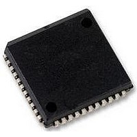
SCC2681AC1A44 NXP Semiconductors, SCC2681AC1A44 Datasheet - Page 3

SCC2681AC1A44
Manufacturer Part Number
SCC2681AC1A44
Description
UART 2-CH 5V 44-Pin PLCC Tube
Manufacturer
NXP Semiconductors
Datasheet
1.SCC2681AC1N40112.pdf
(29 pages)
Specifications of SCC2681AC1A44
Package
44PLCC
Number Of Channels Per Chip
2
Maximum Data Rate
0.1152 MBd
Transmitter And Receiver Fifo Counter
No
Operating Supply Voltage
5 V
Minimum Single Supply Voltage
4.75 V
Maximum Processing Temperature
245 °C
Maximum Supply Current
10 mA
No. Of Channels
2
Uart Features
Quadruple Buffered Receiver Data Register
Supply Voltage Range
4.5V To 5.5V
Operating Temperature Range
0°C To +70°C
Digital Ic Case Style
PLCC
No. Of Pins
44
Data Rate
115.2Kilobaud
Rohs Compliant
Yes
Lead Free Status / RoHS Status
Lead free / RoHS Compliant
Available stocks
Company
Part Number
Manufacturer
Quantity
Price
Company:
Part Number:
SCC2681AC1A44
Manufacturer:
NXP
Quantity:
1 192
Company:
Part Number:
SCC2681AC1A44,512
Manufacturer:
TI
Quantity:
334
Company:
Part Number:
SCC2681AC1A44,512
Manufacturer:
NXP Semiconductors
Quantity:
10 000
Company:
Part Number:
SCC2681AC1A44,518
Manufacturer:
NXP Semiconductors
Quantity:
10 000
Company:
Part Number:
SCC2681AC1A44,529
Manufacturer:
NXP Semiconductors
Quantity:
10 000
Philips Semiconductors
PIN CONFIGURATIONS
PIN DESCRIPTION
2004 Apr 06
SYMBOL
SYMBOL
D0–D7
CEN
WRN
RDN
A0–A3
RESET
INTRN
X1/CLK
Dual asynchronous receiver/transmitter (DUART)
RXDB
TXDB
WRN
GND
OP1
OP3
OP5
OP7
RDN
IP3
IP1
IP0
A0
A1
A2
A3
D1
D3
D5
D7
18
20
10
11
12
13
14
15
16
17
19
1
2
3
4
5
6
7
8
9
PLCC44
2, 4, 6, 7
28, 18,
27, 19,
26, 20,
25, 21
39
10
38
24
36
9
DIP
25, 16,
24, 17,
23, 18,
1, 3, 5,
DIP40
22, 19
PIN
35
34
21
32
8
9
6
40
39
38
37
36
35
34
33
32
31
30
29
28
27
26
25
24
23
22
21
V
IP4
IP5
IP6
IP2
CEN
RESET
X2
X1/CLK
RXDA
TXDA
OP0
OP2
OP4
OP6
D0
D2
D4
D6
INTRN
CC
19, 10,
18, 11,
17, 12,
DIP28
16, 13
1–4
26
25
15
23
5
6
TYPE
TYPE
I/O
O
I
I
I
I
I
I
RXDB
TXDB
WRN
RDN
appropriate frequency (nominally 3.6864 MHz) must be supplied at all times. For crystal
GND
Data Bus: Bidirectional 3-State data bus used to transfer commands, data and status
between the DUART and the CPU. D0 is the least significant bit.
Chip Enable: Active-LOW input signal. When LOW, data transfers between the CPU
and the DUART are enabled on D0-D7 as controlled by the WRN, RDN and A0-A3
inputs. When HIGH, places the D0-D7 lines in the 3-State condition.
Write Strobe: When LOW and CEN is also LOW, the contents of the data bus is
loaded into the addressed register. The transfer occurs on the rising edge of the signal.
Read Strobe: When LOW and CEN is also LOW, causes the contents of the
addressed register to be presented on the data bus. The read cycle begins on the
falling edge of RDN.
Address Inputs: Select the DUART internal registers and ports for read/write
operations.
Reset: A HIGH level clears internal registers (SRA, SRB, IMR, ISR, OPR, OPCR), puts
OP0–OP7 in the HIGH state, stops the counter/timer, and puts Channels A and B in the
inactive state, with the TxDA and TxDB outputs in the mark (HIGH) state. Clears Test
modes, sets MR pointer to MR1.
Interrupt Request: Active-LOW, open-drain, output which signals the CPU that one or
more of the eight maskable interrupting conditions are true.
Crystal 1: Crystal connection or an external clock input. A crystal of a clock the
connections see Figure 7, Clock Timing.
OP1
D7
D3
A0
A1
A3
D1
D5
A2
Figure 1. Pin configurations
10
11
12
13
14
1
2
3
4
5
6
7
8
9
DIP
3
28
27
26
25
24
23
22
21
20
19
18
17
16
15
V
IP2
CEN
RESET
X2
X1/CLK
RXDA
TXDA
OP0
D0
D2
D4
D6
INTRN
CC
NAME AND FUNCTION
NAME AND FUNCTION
CORNER
INDEX
PIN/FUNCTION
17
7
10 RDN
11 RXDB
12 NC
13 TXDB
14 OP1
15 OP3
16 OP5
17 OP7
18 D1
19 D3
20 D5
21 D7
22 GND
1
2
3
4
5
6
7
8
9
18
6
NC
A0
IP3
A1
IP1
A2
A3
IP0
WRN
TOP VIEW
PLCC
1
PIN/FUNCTION
23 NC
24 INTRN
25 D6
26 D4
27 D2
28 D0
29 OP6
30 OP4
31 OP2
32 OP0
33 TXDA
34 NC
35 RXDA
36 X1/CLK
37 X2
38 RESET
39 CEN
40 IP2
41 IP6
42 IP5
43 IP4
44 V
SCC2681
40
28
CC
Product data
39
29
SD00723


