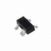
BF991,215 NXP Semiconductors, BF991,215 Datasheet - Page 4

BF991,215
Manufacturer Part Number
BF991,215
Description
MOSFET NCH DUAL GATE 20V SOT143B
Manufacturer
NXP Semiconductors
Datasheet
1.BF991215.pdf
(7 pages)
Specifications of BF991,215
Package / Case
SOT-143, SOT-143B, TO-253AA
Transistor Type
N-Channel Dual Gate
Frequency
100MHz
Gain
29dB
Voltage - Rated
20V
Current Rating
20mA
Noise Figure
0.7dB
Current - Test
10mA
Voltage - Test
10V
Configuration
Single Dual Gate
Continuous Drain Current
0.02 A
Drain-source Breakdown Voltage
20 V
Gate-source Breakdown Voltage
6 V
Maximum Operating Temperature
+ 150 C
Minimum Operating Temperature
- 65 C
Mounting Style
SMD/SMT
Power Dissipation
200 mW
Transistor Polarity
N-Channel
Application
VHF
Channel Type
N
Channel Mode
Depletion
Drain Source Voltage (max)
20V
Power Gain (typ)@vds
29@10VdB
Noise Figure (max)
2dB
Package Type
SOT
Pin Count
3 +Tab
Input Capacitance (typ)@vds
2.1@10V@Gate 1/1@10V@Gate 2pF
Output Capacitance (typ)@vds
1.1@10VpF
Reverse Capacitance (typ)
0.02@10VpF
Operating Temp Range
-65C to 150C
Mounting
Surface Mount
Number Of Elements
1
Power Dissipation (max)
200mW
Screening Level
Military
Lead Free Status / RoHS Status
Lead free / RoHS Compliant
Power - Output
-
Lead Free Status / Rohs Status
Lead free / RoHS Compliant
Other names
568-1970-2
933642000215
BF991 T/R
933642000215
BF991 T/R
NXP Semiconductors
STATIC CHARACTERISTICS
T
DYNAMIC CHARACTERISTICS
Measuring conditions (common source): I
Note
1. Crystal mounted in a SOT103 package.
I
I
I
V
V
V
V
C
C
C
C
F
G
j
G1-SS
G2-SS
DSS
Y
SYMBOL
SYMBOL
= 25 C unless otherwise specified.
(BR)G1-SS
(BR)G2-SS
(P)G1-S
(P)G2-S
ig1-s
ig2-s
rs
os
N-channel dual-gate MOS-FET
tr
fs
gate 1 cut-off current
gate 2 cut-off current
drain current
gate 1-source breakdown voltage I
gate 2-source breakdown voltage I
gate 1-source cut-off voltage
gate 2-source cut-off voltage
transfer admittance
input capacitance at gate 1
input capacitance at gate 2
feedback capacitance
output capacitance
noise figure
transducer gain; note 1
PARAMETER
PARAMETER
D
= 10 mA; V
f = 1 kHz
f = 1 MHz
f = 1 MHz
f = 1 MHz
f = 1 MHz
f = 100 MHz; G
f = 200 MHz; G
f = 100 MHz; G
G
f = 200 MHz; G
G
Rev. 03 - 20 November 2007
L
L
= 0.5 mS; B
= 0.5 mS; B
V
V
V
I
I
G1-SS
G2-SS
D
D
G1-S
G2-S
DS
= 20 A; V
= 20 A; V
DS
= 10 V; V
= 5 V; V
= 5 V; V
= 10 mA; V
= 10 mA; V
= 10 V; V
CONDITIONS
L
L
S
S
S
S
= B
= B
= 1 mS; B
= 2 mS; B
= 1 mS; B
= 2 mS; B
DS
DS
G1-S
CONDITIONS
G2-S
G1-S
Lopt
Lopt
= 10 V; V
= 10 V; V
G2-S
G2-S
G1-S
= 0; V
= V
= V
= 4 V; T
DS
DS
= V
= V
S
S
S
S
G2-S
= B
= B
= B
= B
= 0
= 0
G2-S
G1-S
DS
DS
Sopt
Sopt
Sopt
Sopt
= 0
= 0
= 4 V
amb
= 4 V
= 0
;
;
= 25 C.
10
MIN.
4
6
6
14
2.1
1
20
1.1
0.7
1
29
26
MIN.
TYP.
Product specification
50
50
25
20
20
1.7
2
MAX.
MAX.
2.5
2.5
BF991
4 of 7
nA
nA
mA
V
V
V
V
mS
pF
pF
fF
pF
dB
dB
dB
dB
UNIT
UNIT


