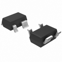
ATF-33143-BLKG Avago Technologies US Inc., ATF-33143-BLKG Datasheet - Page 2

ATF-33143-BLKG
Manufacturer Part Number
ATF-33143-BLKG
Description
IC PHEMT 1.9GHZ 80MA LN SOT-343
Manufacturer
Avago Technologies US Inc.
Datasheet
1.ATF-33143-BLKG.pdf
(18 pages)
Specifications of ATF-33143-BLKG
Package / Case
SC-70-4, SC-82-4, SOT-323-4, SOT-343
Transistor Type
pHEMT FET
Frequency
2GHz
Gain
15dB
Voltage - Rated
5.5V
Current Rating
305mA
Noise Figure
0.5dB
Current - Test
80mA
Voltage - Test
4V
Power - Output
22dBm
Configuration
Single Dual Source
Transistor Polarity
N-Channel
Power Dissipation
600 mW
Drain Source Voltage Vds
5.5 V
Gate-source Breakdown Voltage
- 5 V
Continuous Drain Current
305 mA
Maximum Operating Temperature
+ 160 C
Maximum Drain Gate Voltage
- 5 V
Minimum Operating Temperature
- 65 C
Mounting Style
SMD/SMT
Lead Free Status / RoHS Status
Lead free / RoHS Compliant
Lead Free Status / RoHS Status
Lead free / RoHS Compliant, Lead free / RoHS Compliant
Other names
516-1862
ATF-33143-BLKG
ATF-33143-BLKG
Available stocks
Company
Part Number
Manufacturer
Quantity
Price
Part Number:
ATF-33143-BLKG
Manufacturer:
AVAGO/安华高
Quantity:
20 000
ATF-33143 Absolute Maximum Ratings
Notes:
7. Under large signal conditions, V
8. Distribution data sample size is 450 samples taken from 9 different wafers. Future wafers allocated to this product may have nominal values
9. Measurements made on production test board. This circuit represents a trade-off between an optimal noise match and a realizeable match based
10. The probability of a parameter being between ±1σ is 68.3%, between ±2σ is 95.4% and between ±3σ is 99.7%.
Product Consistency Distribution Charts
2
Figure 1. Typical Pulsed I-V Curves
100
Figure 3. OIP3 @ 2 GHz, 4 V, 80 mA.
LSL=30.0, Nominal=33.3, USL=37.0
500
400
300
200
100
80
60
40
20
P
anywhere within the upper and lower spec limits.
on production test requirements. Circuit losses have been de-embedded from actual measurements.
0
0
29
diss
Symbol
P
0
P
T
in max
V
V
T
V
I
and P
θ
STG
DS
diss
GD
DS
GS
CH
jc
-3 Std
in max
31
2
ratings are not exceeded.
OIP3 (dBm)
Drain - Source Voltage
Gate - Source Voltage
Gate Drain Voltage
Drain Current
Total Power Dissipation
RF Input Power
Channel Temperature
Storage Temperature
Thermal Resistance
V
+0.6 V
DS
33
4
(V)
0 V
[7]
. (V
Parameter
35
GS
GS
6
–0.6 V
= -0.2 V per step)
may swing positive and the drain current may exceed I
[2]
+3 Std
37
[2]
8
[6]
Cpk = 1.21
Std = 0.94
[2]
[5]
[2]
[4]
[1]
[8, 9]
°C/W
Units
dBm
mW
mA
°C
°C
V
V
V
120
100
120
100
Figure 2. NF @ 2 GHz, 4 V, 80 mA.
LSL=0.2, Nominal=0.53, USL=0.8
Figure 4. Gain @ 2 GHz, 4 V, 80 mA.
LSL=13.5, Nominal=14.8, USL=16.5
80
60
40
20
80
60
40
20
0
0
0.2
13
0.3
-65 to 160
Maximum
Absolute
-3 Std
14
-3 Std
I
dss
600
160
145
5.5
20
-5
-5
0.4
[3]
GAIN (dB)
NF (dB)
dss
. These conditions are acceptable as long as the maximum
0.5
15
+3 Std
0.6
Notes:
1. Operation of this device above any one of
2. Assumes DC quiesent conditions.
3. V
4. Source lead temperature is 25°C. Derate
5. Please refer to failure rates in reliability
6. Thermal resistance measured using 150°C
16
+3 Std
0.7
these parameters may cause permanent
damage.
6 mW/°C for T
section to assess the reliability impact
of running devices above a channel
temperature of 140°C.
Liquid Crystal Measurement method.
GS
= 0 V
0.8
17
Cpk = 1.7
Std = 0.05
Cpk = 2.3
Std = 0.2
L
> 60°C.


