ATF-33143-BLKG Avago Technologies US Inc., ATF-33143-BLKG Datasheet - Page 3
ATF-33143-BLKG
Manufacturer Part Number
ATF-33143-BLKG
Description
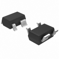
IC PHEMT 1.9GHZ 80MA LN SOT-343
Manufacturer
Avago Technologies US Inc.
Datasheet
1.ATF-33143-BLKG.pdf
(18 pages)
Specifications of ATF-33143-BLKG
Package / Case
SC-70-4, SC-82-4, SOT-323-4, SOT-343
Transistor Type
pHEMT FET
Frequency
2GHz
Gain
15dB
Voltage - Rated
5.5V
Current Rating
305mA
Noise Figure
0.5dB
Current - Test
80mA
Voltage - Test
4V
Power - Output
22dBm
Configuration
Single Dual Source
Transistor Polarity
N-Channel
Power Dissipation
600 mW
Drain Source Voltage Vds
5.5 V
Gate-source Breakdown Voltage
- 5 V
Continuous Drain Current
305 mA
Maximum Operating Temperature
+ 160 C
Maximum Drain Gate Voltage
- 5 V
Minimum Operating Temperature
- 65 C
Mounting Style
SMD/SMT
Lead Free Status / RoHS Status
Lead free / RoHS Compliant
Lead Free Status / RoHS Status
Lead free / RoHS Compliant, Lead free / RoHS Compliant
Other names
516-1862
ATF-33143-BLKG
ATF-33143-BLKG
Available stocks
Company
Part Number
Manufacturer
Quantity
Price

Part Number:
ATF-33143-BLKG
Manufacturer:
AVAGO/安华高
Quantity:
20 000


ATF-33143 DC Electrical Specifications
Notes:
1. Guaranteed at wafer probe level.
2. Typical value determined from a sample size of 450 parts from 9 wafers.
3. Measurements obtained using production test board described in Figure 5.
Input
Figure 5. Block diagram of 2 GHz production test board used for Noise Figure, Associated Gain, P1dB, and OIP3 measurements. This circuit represents a
trade-off between an optimal noise match and a realizable match based on production test requirements. Circuit losses have been de-embedded from
actual measurements.
3
Symbol
I
g
OIP3
V
I
P
dss
GDO
I
NF
G
P
m
gss
I
1dB
d
[1]
a
[1]
[1]
Line Including
Transmission
(0.5 dB loss)
Gate Bias T
50 Ohm
Parameters and Test Conditions
Saturated Drain Current
Pinchoff Voltage
Quiescent Bias Current
Transconductance
Gate to Drain Leakage Current
Gate Leakage Current
Noise Figure
Associated Gain
Output 3
Intercept Point
1 dB Compressed
Compressed Power
rd
Order
Matching Circuit
[3]
Γ_mag = 0.20
Γ_ang = 124°
[3]
(0.3 dB loss)
[3]
Input
T
A
5 dBm Pout/Tone
5 dBm Pout/Tone
= 25°C, RF parameters measured in a test circuit for a typical device
f = 900 MHz
f = 900 MHz
f = 900 MHz
f = 900 MHz
f = 2 GHz
f = 2 GHz
f = 2 GHz
f = 2 GHz
DUT
V
DS
= 1.5 V, I
V
DS
V
V
V
V
V
V
V
V
V
V
V
V
V
V
V
V
V
DS
DS
DS
DS
DS
DS
DS
DS
DS
DS
DS
DS
DS
DS
DS
DS
V
= 1.5 V, g
GS
DS
= 4 V, I
= 4 V, I
= 4 V, I
= 4 V, I
= 4 V, I
= 4 V, I
= 4 V, I
= 4 V, I
= 4 V, I
= 4 V, I
= 4 V, I
= 4 V, I
= 4 V, I
= 4 V, I
= 4 V, I
= 4 V, I
= -0.5 V, V
= 1.5 V, V
Line Including
V
Transmission
(0.5 dB loss)
Drain Bias T
DS
GD
= 10% of I
50 Ohm
= V
DS
DS
DS
DS
DS
DS
DS
DS
DS
DS
DS
DS
DS
DS
DS
DS
m
V
= 80 mA
= 60 mA
= 80 mA
= 60 mA
= 80 mA
= 60 mA
= 80 mA
= 60 mA
= 80 mA
= 60 mA
= 80 mA
= 60 mA
= 80 mA
= 60 mA
= 80 mA
= 60 mA
= I
GS
GD
DS
GS
= -4 V
dss
= 0 V
= 4 V
= 5 V
/V
dss
P
Output
mmho 360
Units
dBm
dBm
dBm
dBm
mA
mA
µA
µA
dB
dB
dB
dB
V
-0.65
13.5
Min. Typ.
175
—
—
30
33.5
32.5
-0.5
237
440
0.5
0.5
0.4
0.4
80
42
15
15
21
21
32
31
22
21
21
20
[2]
-0.35
1000
16.5
Max.
305
600
0.8
—
—
Related parts for ATF-33143-BLKG
Image
Part Number
Description
Manufacturer
Datasheet
Request
R

Part Number:
Description:
IC PHEMT 1.9GHZ 80MA LN SOT-343
Manufacturer:
Avago Technologies US Inc.
Datasheet:

Part Number:
Description:
TRANSISTOR,HEMT,N-CHAN,5.5V V(BR)DSS,175mA I(DSS),SOT-343R
Manufacturer:
Avago Technologies US Inc.
Part Number:
Description:
IC PHEMT 1.9GHZ 80MA LN SOT-343
Manufacturer:
Avago Technologies US Inc.
Datasheet:

Part Number:
Description:
RF Bipolar Transistor
Manufacturer:
Avago Technologies US Inc.
Part Number:
Description:
TRANSISTOR,HEMT,N-CHAN,5.5V V(BR)DSS,175mA I(DSS),SOT-343R
Manufacturer:
Avago Technologies US Inc.

Part Number:
Description:
OPTOCOUPLER GATE DRV 2A 16-SOIC
Manufacturer:
Avago Technologies US Inc.
Datasheet:
Part Number:
Description:
OPTOCOUPLER 2CH 2.5A 16-SOIC
Manufacturer:
Avago Technologies US Inc.
Datasheet:

Part Number:
Description:
OPTOCOUPLER GATE DRV 0.4A 16SOIC
Manufacturer:
Avago Technologies US Inc.
Datasheet:

Part Number:
Description:
OPTOCOUPLER 2.0A 250KHZ 8-DIP
Manufacturer:
Avago Technologies US Inc.
Datasheet:

Part Number:
Description:
OPTOCOUPLER 2.0A 250KHZ GW 8-SMD
Manufacturer:
Avago Technologies US Inc.
Datasheet:

Part Number:
Description:
OPTOCOUPLER 2CH 15MBD 3.3V 8SOIC
Manufacturer:
Avago Technologies US Inc.
Datasheet:
Part Number:
Description:
OPTOCOUPLER DARL-OUT 8-DIP
Manufacturer:
Avago Technologies US Inc.
Datasheet:
Part Number:
Description:
OPTOCOUPLER IGBT DRIVE 0.4A 8DIP
Manufacturer:
Avago Technologies US Inc.
Datasheet:
Part Number:
Description:
OPTOCOUPLER DARL-OUT 8-DIP
Manufacturer:
Avago Technologies US Inc.
Datasheet:

Part Number:
Description:
OPTOCOUPLER 1CH 1MBS 8-SMD GW
Manufacturer:
Avago Technologies US Inc.
Datasheet: