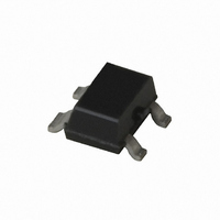
ATF-54143-BLKG Avago Technologies US Inc., ATF-54143-BLKG Datasheet

ATF-54143-BLKG
Specifications of ATF-54143-BLKG
ATF-54143-BLKG
Available stocks
Related parts for ATF-54143-BLKG
ATF-54143-BLKG Summary of contents
Page 1
... ESD Machine Model (Class A) ESD Human Body Model (Class 1A) Refer to Agilent Application Note A004R: Electrostatic Discharge Damage and Control. Agilent ATF-54143 Low Noise Enhancement Mode Pseudomorphic HEMT in a Surface Mount Plastic Package Data Sheet Surface Mount Package ...
Page 2
... ATF-54143 Absolute Maximum Ratings Symbol Parameter [2] V Drain - Source Voltage DS [2] V Gate - Source Voltage GS [2] V Gate Drain Voltage GD [2] I Drain Current DS [3] P Total Power Dissipation diss P RF Input Power in max. I Gate Source Current GS T Channel Temperature CH T Storage Temperature STG [4] θ ...
Page 3
... ATF-54143 Electrical Specifications T = 25°C, RF parameters measured in a test circuit for a typical device A Symbol Parameter and Test Condition Vgs Operational Gate Voltage Vth Threshold Voltage Idss Saturated Drain Current Gm Transconductance Igss Gate Leakage Current [1] NF Noise Figure [1] Ga Associated Gain OIP3 ...
Page 4
... ATF-54143 Typical Performance Curves 0.7 0.6 0.5 0.4 3V 0 100 I (mA) ds Figure 6. Fmin vs. I and V Tuned for ds ds Max OIP3 and Fmin at 2 GHz 100 I (mA) ds Figure 9. Gain vs. I and V Tuned for ds ds Max OIP3 and Fmin at 900 MHz 100 ...
Page 5
... Tuned for Max OIP3 and Fmin at 3V, 60 mA. 1.4 1.2 1.0 0.8 0 FREQUENCY (GHz) [1] Figure 18. Fmin vs. Frequency and 3V. ATF-54143 Reflection Coefficient Parameters tuned for Maximum Output IP3 3V [1] Freq ΓOut_Mag. ΓOut_Ang. (GHz) (Mag) (Degrees) 0.9 0.017 115 2.0 0.026 -85 3.9 0.013 173 5.8 0.025 102 Note: 1 ...
Page 6
... ATF-54143 Typical Scattering Parameters, V Freq GHz Mag. Ang. dB 0.1 0.99 -17.6 27.99 0.5 0.83 -76.9 25.47 0.9 0.72 -114 22.52 1.0 0.70 -120.6 21.86 1.5 0.65 -146.5 19.09 1.9 0.63 -162.1 17.38 2.0 0.62 -165.6 17.00 2.5 0.61 178.5 15.33 3.0 ...
Page 7
... ATF-54143 Typical Scattering Parameters, V Freq GHz Mag. Ang. dB 0.1 0.99 -18.9 28.84 0.5 0.81 -80.8 26.04 0.9 0.71 -117.9 22.93 1.0 0.69 -124.4 22.24 1.5 0.64 -149.8 19.40 1.9 0.62 -164.9 17.66 2.0 0.62 -168.3 17.28 2.5 0.60 176.2 15.58 3.0 ...
Page 8
... ATF-54143 Typical Scattering Parameters, V Freq GHz Mag. Ang. dB 0.1 0.98 -20.4 28.32 0.5 0.80 -85.9 25.32 0.9 0.72 -123.4 22.10 1.0 0.70 -129.9 21.40 1.5 0.66 -154.6 18.55 1.9 0.65 -169.5 16.81 2.0 0.64 -172.8 16.42 2.5 0.64 172.1 14.69 3.0 ...
Page 9
... ATF-54143 Typical Scattering Parameters, V Freq GHz Mag. Ang. dB 0.1 0.99 -18.6 28.88 0.5 0.81 -80.2 26.11 0.9 0.71 -117.3 23.01 1.0 0.69 -123.8 22.33 1.5 0.64 -149.2 19.49 1.9 0.62 -164.5 17.75 2.0 0.61 -167.8 17.36 2.5 0.60 176.6 15.66 3.0 ...
Page 10
... Figure 1. Typical ATF-54143 LNA with Passive Biasing. Capacitors C2 and C5 provide a low impedance in-band RF bypass for the matching net- works. Resistors R3 and R4 provide a very important low frequency termination for the device. The resistive termination improves low frequency stability. Capacitors C3 and C6 provide the low frequency RF bypass for resistors R3 and R4 ...
Page 11
... Figure 2. Typical ATF-54143 LNA with Active Biasing. An active bias scheme is shown in Figure 2. R1 and R2 provide a constant voltage source at the base of a PNP transistor at Q2. The constant voltage at the base raised by 0.7 volts at the emitter. The constant emitter voltage plus the regulated V ...
Page 12
... Tau= Rgd=0.25 Ohm Tnom=16.85 Rd=1.0125 Ohm Idstc= Ucrit=-0.72 Rg=1.0 Ohm Vgexp=1.91 Rs=0.3375 Ohm Gamds=1e-4 Ld= Vtotc= Lg=0.18 nH Betatce= Ls= Rgs=0.25 Ohm Cds=0.27 pF Rc=250 Ohm ATF-54143 curtice ADS Model INSIDE Package VAR Var Egn VAR1 K=5 Z2=85 Z1= GATE C=0.13 pF Port TLINP TLINP G TL4 ...
Page 13
... V2 D=20.0 mil H=25.0 mil T=0.15 mil Rho=1.0 W=40.0 mil Figure 3. Adding Vias to the ATF-54143 Non-Linear Model for Comparison to Measured S and Noise Parameters. 13 eters and the simulated non- linear model, be sure to include the effect of the printed circuit board to get an accurate compari- son. This is shown schematically in Figure 3 ...
Page 14
Noise Parameter Applications Information F values at 2 GHz and higher min are based on measurements while the F below 2 GHz have mins been extrapolated. The F min values are based on a set of 16 noise figure measurements ...
Page 15
... Ordering Information Part Number No. of Devices ATF-54143-TR1 ATF-54143-TR2 ATF-54143-BLK ATF-54143-TR1G ATF-54143-TR2G ATF-54143-BLKG Note: For lead-free option, the part number will have the characger "G" at the end. Package Dimensions Outline 43 (SO%-343/SC70 4 lead) Symbol Min (mm) E 1.15 D 1.85 HE 1.80 A 0.80 A2 0. ...
Page 16
Recommended PCB Pad Layout for Agilent's SC70 4L/SOT-343 Products (dimensions in inches/mm) Device Orientation REEL CARRIER TAPE USER FEED DIRECTION COVER TAPE 16 TOP VIEW END VIEW ...
Page 17
Tape Dimensions and Product Orientation Description Cavity Length Width Depth Pitch Bottom Hole Diameter Perforlation Diameter Pitch Position Carrier Tape Width Thickness Cover Tape Width Thickness Distance Cavity to Perforation (Width Direction) Cavity to Perforation (Length Direction) For product information ...


