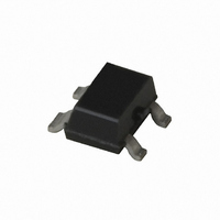
ATF-54143-BLKG Avago Technologies US Inc., ATF-54143-BLKG Datasheet - Page 4

ATF-54143-BLKG
Manufacturer Part Number
ATF-54143-BLKG
Description
IC PHEMT 2GHZ 3V 60MA SOT-343
Manufacturer
Avago Technologies US Inc.
Datasheet
1.ATF-54143-TR2G.pdf
(17 pages)
Specifications of ATF-54143-BLKG
Package / Case
SC-70-4, SC-82-4, SOT-323-4, SOT-343
Transistor Type
pHEMT FET
Frequency
2GHz
Gain
16.6dB
Voltage - Rated
5V
Current Rating
120mA
Noise Figure
0.5dB
Current - Test
60mA
Voltage - Test
3V
Power - Output
20.4dBm
Configuration
Single Dual Source
Transistor Polarity
N-Channel
Power Dissipation
725 mW
Drain Source Voltage Vds
5 V
Gate-source Breakdown Voltage
- 5 V to 1 V
Continuous Drain Current
120 mA
Maximum Operating Temperature
+ 150 C
Maximum Drain Gate Voltage
- 5 V to 1 V
Minimum Operating Temperature
- 65 C
Mounting Style
SMD/SMT
Continuous Drain Current Id
120mA
Power Dissipation Pd
725mW
Noise Figure Typ
0.5dB
Rf Transistor Case
SOT-343
No. Of Pins
4
Frequency Max
6GHz
Rohs Compliant
Yes
Drain Current Idss Max
60mA
Lead Free Status / RoHS Status
Lead free / RoHS Compliant
Lead Free Status / RoHS Status
Lead free / RoHS Compliant, Lead free / RoHS Compliant
Other names
516-1868
ATF-54143-BLKG
ATF-54143-BLKG
Available stocks
Company
Part Number
Manufacturer
Quantity
Price
Company:
Part Number:
ATF-54143-BLKG
Manufacturer:
AVAGO
Quantity:
30 000
Part Number:
ATF-54143-BLKG
Manufacturer:
AVAGO/安华高
Quantity:
20 000
ATF-54143 Typical Performance Curves
Notes:
1. I
2. Fmin values at 2 GHz and higher are based on
4
Figure 9. Gain vs. I
Max OIP3 and Fmin at 900 MHz.
Figure 6. Fmin vs. I
Max OIP3 and Fmin at 2 GHz.
Figure 12. P1dB vs. I
Max OIP3 and Fmin at 2 GHz.
0.7
0.6
0.5
0.4
0.3
0.2
25
24
23
22
21
20
19
18
24
22
20
18
16
14
12
without RF drive applied. Under low values of
I
increase substantially as P1dB is approached.
measurements while the Fmins below 2 GHz
have been extrapolated. The Fmin values are
dq
ds
0
0
0
, the application of RF drive will cause I
represents the quiescent drain current
20
20
20
I
40
40
40
ds
dq
I
ds
I
ds
ds
dq
(mA)
and V
and V
(mA)
(mA)
and V
[1]
60
60
60
ds
ds
ds
Tuned for
Tuned for
Tuned for
80
80
80
3V
4V
3V
4V
3V
4V
100
100
100
d
to
Figure 7. Fmin vs. I
Max OIP3 and Min NF at 900 MHz.
Figure 13. P1dB vs. I
Max OIP3 and Fmin at 900 MHz.
Figure 10. OIP3 vs. I
Max OIP3 and Fmin at 2 GHz.
based on a set of 16 noise figure measure-
ments made at 16 different impedances using
an ATN NP5 test system. From these
measurements a true Fmin is calculated.
Refer to the noise parameter application
section for more information.
0.6
0.5
0.4
0.3
0.2
0.1
23
22
21
20
19
18
17
16
15
42
37
32
27
22
17
12
0
0
0
0
20
20
20
I
40
40
40
dq
I
ds
I
ds
ds
ds
dq
(mA)
and V
(mA)
(mA)
and V
and V
[1]
60
60
60
ds
ds
ds
Tuned for
Tuned for
Tuned for
80
80
80
3V
4V
3V
4V
3V
4V
100
100
100
Figure 8. Gain vs. I
Max OIP3 and Fmin at 2 GHz.
Figure 11. OIP3 vs. I
Max OIP3 and Fmin at 900 MHz.
Figure 14. Gain vs. Frequency and Temp
Tuned for Max OIP3 and Fmin at 3V, 60 mA.
19
18
17
16
15
14
13
12
40
35
30
25
20
15
35
30
25
20
15
10
5
0
0
0
1
20
20
FREQUENCY (GHz)
2
40
40
ds
I
I
ds
ds
ds
and V
(mA)
(mA)
3
and V
60
60
ds
ds
4
Tuned for
Tuned for
80
80
25°C
-40°C
85°C
5
3V
4V
3V
4V
100
100
6


