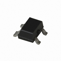
ATF-54143-BLKG Avago Technologies US Inc., ATF-54143-BLKG Datasheet - Page 11

ATF-54143-BLKG
Manufacturer Part Number
ATF-54143-BLKG
Description
IC PHEMT 2GHZ 3V 60MA SOT-343
Manufacturer
Avago Technologies US Inc.
Datasheet
1.ATF-54143-TR2G.pdf
(17 pages)
Specifications of ATF-54143-BLKG
Package / Case
SC-70-4, SC-82-4, SOT-323-4, SOT-343
Transistor Type
pHEMT FET
Frequency
2GHz
Gain
16.6dB
Voltage - Rated
5V
Current Rating
120mA
Noise Figure
0.5dB
Current - Test
60mA
Voltage - Test
3V
Power - Output
20.4dBm
Configuration
Single Dual Source
Transistor Polarity
N-Channel
Power Dissipation
725 mW
Drain Source Voltage Vds
5 V
Gate-source Breakdown Voltage
- 5 V to 1 V
Continuous Drain Current
120 mA
Maximum Operating Temperature
+ 150 C
Maximum Drain Gate Voltage
- 5 V to 1 V
Minimum Operating Temperature
- 65 C
Mounting Style
SMD/SMT
Continuous Drain Current Id
120mA
Power Dissipation Pd
725mW
Noise Figure Typ
0.5dB
Rf Transistor Case
SOT-343
No. Of Pins
4
Frequency Max
6GHz
Rohs Compliant
Yes
Drain Current Idss Max
60mA
Lead Free Status / RoHS Status
Lead free / RoHS Compliant
Lead Free Status / RoHS Status
Lead free / RoHS Compliant, Lead free / RoHS Compliant
Other names
516-1868
ATF-54143-BLKG
ATF-54143-BLKG
Available stocks
Company
Part Number
Manufacturer
Quantity
Price
Company:
Part Number:
ATF-54143-BLKG
Manufacturer:
AVAGO
Quantity:
30 000
Part Number:
ATF-54143-BLKG
Manufacturer:
AVAGO/安华高
Quantity:
20 000
The values of resistors R1 and R2
are calculated with the following
formulas
R1 =
R2 =
Example Circuit
V
V
I
V
Choose I
normal expected gate leakage
current. I
2 mA for this example. Using
equations (1), (2), and (3) the
resistors are calculated as
follows
R1 = 295Ω
R2 = 1205Ω
R3 = 32.3Ω
Active Biasing
Active biasing provides a means
of keeping the quiescent bias
point constant over temperature
and constant over lot to lot
variations in device dc perfor-
mance. The advantage of the
active biasing of an enhancement
mode PHEMT versus a depletion
mode PHEMT is that a negative
power source is not required. The
techniques of active biasing an
enhancement mode device are
very similar to those used to bias
a bipolar junction transistor.
11
ds
DD
ds
gs
= 60 mA
= 0.59V
= 3V
= 5 V
V
(V
I
gs
BB
ds
BB
BB
p
– V
to be at least 10X the
V
was chosen to be
(2)
gs
gs
) R1
p
(3)
INPUT
Figure 2. Typical ATF-54143 LNA with
Active Biasing.
An active bias scheme is shown
in Figure 2. R1 and R2 provide a
constant voltage source at the
base of a PNP transistor at Q2.
The constant voltage at the base
of Q2 is raised by 0.7 volts at the
emitter. The constant emitter
voltage plus the regulated V
supply are present across resis-
tor R3. Constant voltage across
R3 provides a constant current
supply for the drain current.
Resistors R1 and R2 are used to
set the desired Vds. The com-
bined series value of these
resistors also sets the amount of
extra current consumed by the
bias network. The equations that
describe the circuit’s operation
are as follows.
V
R3 =
V
V
V
Rearranging equation (4)
provides the following formula
R2 =
E
B
B
DD
= V
=
= V
Zo
= I
R7
V
E
ds
R
R1 + R2
BB
R5
R6
C1
DD
– V
L1
1
+ (I
R1
(V
(R1 + R2)
– V
I
R1
C3
ds
C2
BE
DD
V
ds
E
B
Q1
L2
•
p
– V
p
C7
V
Q2
R4)
DD
B
)
L3
R2
p
L4
C5
R4
C6
(5)
(1)
(4A)
(3)
(2)
(4)
C4
R3
Zo
DD
OUTPUT
Vdd
and rearranging equation (5)
provides the following formula
R1 =
Example Circuit
V
V
I
R4 = 10Ω
V
Equation (1) calculates the
required voltage at the emitter of
the PNP transistor based on
desired V
resistor R4 to be 3.6V. Equation
(2) calculates the value of resis-
tor R3 which determines the
drain current I
R3 =23.3Ω. Equation (3) calcu-
lates the voltage required at the
junction of resistors R1 and R2.
This voltage plus the step-up of
the base emitter junction deter-
mines the regulated V
tions (4) and (5) are solved
simultaneously to determine the
value of resistors R1 and R2. In
the example R1=1450Ω and
R2 =1050Ω. R7 is chosen to be
1kΩ. This resistor keeps a small
amount of current flowing
through Q2 to help maintain bias
stability. R6 is chosen to be
10kΩ. This value of resistance is
necessary to limit Q1 gate
current in the presence of high
RF drive level (especially when
Q1 is driven to P
pression point).
ds
DD
ds
BE
= 60 mA
= 3V
= 5V
= 0.7 V
I
BB
ds
(
1 +
and I
V
DD
ds
V
. In the example
1dB
DD
ds
V
– V
through
gain com-
B
ds
B
. Equa-
)
p
9
(5A)


