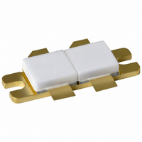
BLF278,112 NXP Semiconductors, BLF278,112 Datasheet - Page 6

BLF278,112
Manufacturer Part Number
BLF278,112
Description
TRANSISTOR RF DMOS SOT262A1
Manufacturer
NXP Semiconductors
Datasheet
1.BLF278112.pdf
(23 pages)
Specifications of BLF278,112
Package / Case
SOT-262A1
Transistor Type
2 N-Channel (Dual)
Frequency
108MHz
Gain
22dB
Voltage - Rated
125V
Current Rating
18A
Current - Test
100mA
Voltage - Test
50V
Power - Output
300W
Minimum Operating Temperature
- 65 C
Mounting Style
SMD/SMT
Resistance Drain-source Rds (on)
0.3 Ohm @ 10 V
Transistor Polarity
N-Channel
Configuration
Dual Common Source
Drain-source Breakdown Voltage
125 V
Gate-source Breakdown Voltage
+/- 20 V
Continuous Drain Current
18 A
Power Dissipation
500000 mW
Maximum Operating Temperature
+ 200 C
Application
VHF
Channel Type
N
Channel Mode
Enhancement
Drain Source Voltage (max)
125V
Power Gain (typ)@vds
20(Min)@50V/18@50V/16@50VdB
Frequency (max)
225MHz
Package Type
CDFM
Pin Count
5
Forward Transconductance (typ)
6.2S
Drain Source Resistance (max)
300@10Vmohm
Input Capacitance (typ)@vds
480@50VpF
Output Capacitance (typ)@vds
190@50VpF
Reverse Capacitance (typ)
14@50VpF
Operating Temp Range
-65C to 200C
Drain Efficiency (typ)
80%
Mounting
Screw
Mode Of Operation
CW Class-AB/CW Class-B/CW Class-C
Number Of Elements
2
Power Dissipation (max)
500000mW
Vswr (max)
7
Screening Level
Military
Lead Free Status / RoHS Status
Lead free / RoHS Compliant
Noise Figure
-
Lead Free Status / Rohs Status
Lead free / RoHS Compliant
Other names
568-2412
933978520112
BLF278
BLF278
933978520112
BLF278
BLF278
Philips Semiconductors
APPLICATION INFORMATION
Class-B operation
RF performance in CW operation in a common source push-pull test circuit. T
otherwise specified. R
Ruggedness in class-B operation
The BLF278 is capable of withstanding a load mismatch corresponding to VSWR = 7:1 through all phases under the
following conditions: V
2003 Sep 19
handbook, halfpage
CW, class-B
CW, class-C
VHF push-pull power MOS transistor
V
Fig.8
(pF)
C rs
GS
MODE OF OPERATION
400
300
200
100
= 0; f = 1 MHz.
0
0
Feedback capacitance as a function of
drain-source voltage; typical values per
section.
10
GS
DS
20
= 4
= 50 V; f = 108 MHz at rated load power.
per section; optimum load impedance per section = 3.2 + j4.3
30
(MHz)
108
108
40
f
V DS (V)
MGE620
50
V
(V)
50
50
DS
6
V
2
GS
I
(A)
DQ
0.1
= 0
300
300
(W)
P
h
L
= 25 C; R
th mb-h
typ. 22
typ. 18
(dB)
G
20
p
(V
= 0.15 K/W unless
Product Specification
DS
= 50 V).
BLF278
typ. 70
typ. 80
>60
(%)
D


