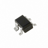
BF904WR,115 NXP Semiconductors, BF904WR,115 Datasheet

BF904WR,115
Specifications of BF904WR,115
Related parts for BF904WR,115
BF904WR,115 Summary of contents
Page 1
DATA SHEET BF904WR N-channel dual-gate MOS-FET Product specification Supersedes data of 1995 Apr 25 DISCRETE SEMICONDUCTORS 2010 Sep 15 ...
Page 2
... NXP Semiconductors N-channel dual-gate MOS-FET FEATURES Specially designed for use supply voltage Short channel transistor with high forward transfer admittance to input capacitance ratio Low noise gain controlled amplifier GHz Superior cross-modulation performance during AGC. APPLICATIONS VHF and UHF applications with supply voltage such as television tuners and professional communications equipment ...
Page 3
... NXP Semiconductors N-channel dual-gate MOS-FET LIMITING VALUES In accordance with the Absolute Maximum Rating System (IEC 134). SYMBOL PARAMETER V drain-source voltage DS I drain current D I gate 1 current G1 I gate 2 current G2 P total power dissipation tot T storage temperature stg T operating junction temperature j Note 1 ...
Page 4
... NXP Semiconductors N-channel dual-gate MOS-FET THERMAL CHARACTERISTICS SYMBOL R thermal resistance from junction to ambient th j-a R thermal resistance from junction to soldering point th j-s Notes 1. Device mounted on a printed-circuit board the temperature at the soldering point of the source lead. s STATIC CHARACTERISTICS = 25 C; unless otherwise specified. ...
Page 5
... NXP Semiconductors N-channel dual-gate MOS-FET (mS Fig.3 Forward transfer admittance as a function of junction temperature; typical values. 120 handbook, halfpage V unw μ (dB V) 110 100 MHz MHz 120 k unw amb G1 Fig.5 Unwanted voltage for 1% cross-modulation as a function of gain reduction; typical values ...
Page 6
... NXP Semiconductors N-channel dual-gate MOS-FET 20 handbook, halfpage (mA) 16 1 1 Fig.7 Output characteristics; typical values. 40 handbook, halfpage y fs (mS Fig.9 Forward transfer admittance as a function of drain current; typical values. 2010 Sep 15 MLD269 handbook, halfpage = 1 (V) DS MLD272 handbook, halfpage ...
Page 7
... NXP Semiconductors N-channel dual-gate MOS-FET 12 handbook, halfpage I D (mA G2 120 k (connected Fig.11 Drain current as a function of gate 1 supply voltage (= V see Fig.19. 12 handbook, halfpage I D (mA 120 k (connected Fig.13 Drain current as a function of gate 2 voltage; typical values; see Fig.19. ...
Page 8
... NXP Semiconductors N-channel dual-gate MOS-FET 2 10 handbook, halfpage y is (mS mA amb Fig.15 Input admittance as a function of frequency; typical values (mS) ϕ mA amb Fig.17 Forward transfer admittance and phase as a function of frequency; typical values. 2010 Sep 15 MLD277 (MHz) MLD279 2 10 handbook, halfpage ϕ ...
Page 9
... NXP Semiconductors N-channel dual-gate MOS-FET R GEN 2010 Sep 15 V AGC Ω Ω Ω Fig.19 Cross-modulation test set-up. 9 Product specification DUT 50 Ω ≈ 450 nH C4 4.7 nF MLD171 V DS BF904WR ...
Page 10
... NXP Semiconductors N-channel dual-gate MOS-FET Table 1 Scattering parameters MAGNITUDE ANGLE (MHz) (ratio) (deg) 3.4 40 0.989 8.3 100 0.985 16.4 200 0.976 24.1 300 0.958 32.0 400 0.942 39.3 500 0.918 46.0 600 0.899 52.6 700 0.876 58.8 800 0.852 64.9 900 0.823 ...
Page 11
... NXP Semiconductors N-channel dual-gate MOS-FET PACKAGE OUTLINE Plastic surface-mounted package; reverse pinning; 4 leads DIMENSIONS (mm are the original dimensions UNIT max 0.4 0.7 1.1 mm 0.1 0.8 0.3 0.5 OUTLINE VERSION IEC SOT343R 2010 Sep scale 0.25 2.2 1.35 1.3 1.15 0.10 1.8 1 ...
Page 12
... In no event shall NXP Semiconductors be liable for any indirect, incidental, punitive, special or consequential damages (including - without limitation - lost profits, lost savings, business interruption, costs related to the ...
Page 13
... NXP Semiconductors’ specifications such use shall be solely at customer’s own risk, and (c) customer fully indemnifies NXP Semiconductors for any liability, damages or failed product claims resulting from customer design and use of the product for automotive applications beyond NXP Semiconductors’ ...
Page 14
... Interface, Security and Digital Processing expertise Customer notification This data sheet was changed to reflect the new company name NXP Semiconductors, including new legal definitions and disclaimers. No changes were made to the technical content, except for the marking codes and the package outline drawings which were updated to the latest version. ...


