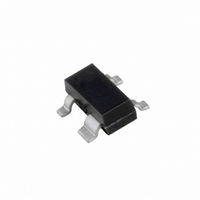
BF1211R,215 NXP Semiconductors, BF1211R,215 Datasheet - Page 9

BF1211R,215
Manufacturer Part Number
BF1211R,215
Description
MOSFET N-CH DUAL GATE 6V SOT143R
Manufacturer
NXP Semiconductors
Datasheet
1.BF1211215.pdf
(16 pages)
Specifications of BF1211R,215
Package / Case
SC-61B
Transistor Type
N-Channel Dual Gate
Frequency
400MHz
Gain
29dB
Voltage - Rated
6V
Current Rating
30mA
Noise Figure
0.9dB
Current - Test
15mA
Voltage - Test
5V
Minimum Operating Temperature
- 65 C
Mounting Style
SMD/SMT
Transistor Polarity
N-Channel
Configuration
Single Dual Gate
Drain-source Breakdown Voltage
6 V
Gate-source Breakdown Voltage
6 V
Continuous Drain Current
30 mA
Power Dissipation
180 mW
Maximum Operating Temperature
+ 150 C
Lead Free Status / RoHS Status
Lead free / RoHS Compliant
Power - Output
-
Lead Free Status / Rohs Status
Lead free / RoHS Compliant
Other names
568-1960-2
934057512215
BF1211R
934057512215
BF1211R
NXP Semiconductors
2003 Dec 16
handbook, halfpage
handbook, halfpage
N-channel dual-gate MOS-FETs
V
I
Fig.17 Input admittance as a function of frequency;
V
I
Fig.19 Forward transfer admittance and phase as
D
D
DS
DS
(mS)
(mS)
|y fs |
= 15 mA; T
= 15 mA; T
y is
10
10
10
= 5 V; V
= 5 V; V
10
10
−1
1
1
2
2
10
10
typical values.
functions of frequency; typical values.
G2
G2
amb
amb
= 4 V.
= 4 V.
= 25 C.
= 25 C.
10
10
2
2
b is
|y fs |
g is
ϕ fs
f (MHz)
f (MHz)
MDB841
MDB843
10
10
3
3
−10
−10
−1
(deg)
ϕ fs
2
9
handbook, halfpage
handbook, halfpage
V
I
Fig.18 Reverse transfer admittance and phase as
Fig.20 Output admittance as a function of
V
I
D
D
DS
(mS)
DS
(μS)
|y rs |
y os
= 15 mA; T
= 15 mA; T
10
10
10
10
= 5 V; V
= 5 V; V
10
10
−1
−2
BF1211; BF1211R; BF1211WR
1
1
3
2
10
10
a function of frequency; typical values.
frequency; typical values.
G2
G2
amb
amb
= 4 V.
= 4 V.
= 25 C.
= 25 C.
10
10
2
2
b os
g os
ϕ rs
|y rs |
f (MHz)
f (MHz)
Product specification
MDB842
MDB844
10
10
3
3
−10
−10
−10
−1
(deg)
ϕ rs
3
2


