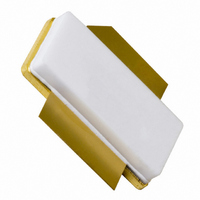
BLF6G10LS-200,112 NXP Semiconductors, BLF6G10LS-200,112 Datasheet

BLF6G10LS-200,112
Specifications of BLF6G10LS-200,112
BLF6G10LS-200
BLF6G10LS-200
Related parts for BLF6G10LS-200,112
BLF6G10LS-200,112 Summary of contents
Page 1
... BLF6G10LS-200 Power LDMOS transistor Rev. 01 — 18 January 2008 1. Product profile 1.1 General description 200 W LDMOS power transistor for base station applications at frequencies from 800 MHz to 1000 MHz. Table 1. Typical RF performance at T Mode of operation 2-carrier W-CDMA [1] Test signal: 3GPP; test model 1; 64 DPCH; PAR = 7 0.01 % probability on CCDF per carrier; carrier spacing 5 MHz ...
Page 2
... RF power amplifiers for GSM, GSM EDGE, W-CDMA and CDMA base stations and multicarrier applications in the 800 MHz to 1000 MHz frequency range. 2. Pinning information Table 2. Pin [1] Connected to flange 3. Ordering information Table 3. Type number BLF6G10LS-200 - 4. Limiting values Table 4. In accordance with the Absolute Maximum Rating System (IEC 60134). Symbol stg ...
Page 3
... RF performance at V class-AB production test circuit. Symbol P L(AV ACPR 7.1 Ruggedness in class-AB operation The BLF6G10LS-200 is capable of withstanding a load mismatch corresponding to VSWR = through all phases under the following conditions 1400 mA BLF6G10LS-200_1 Preliminary data sheet Characteristics Conditions drain-source breakdown V voltage gate-source threshold voltage ...
Page 4
... 1400 mA 894 MHz typical values (dB 100 1400 mA 893.95 MHz power; typical values Rev. 01 — 18 January 2008 BLF6G10LS-200 Power LDMOS transistor 001aah526 70 D (%) 120 160 200 240 P (W) L 001aah534 60 D (%) 150 200 250 300 350 P (W) L(PEP) = 894.05 MHz. 2 © NXP B.V. 2008. All rights reserved. ...
Page 5
... MHz (5) 1500 MHz Fig 4. Third order intermodulation distortion as a 001aah537 50 D ACPR (%) (dBc (W) L(AV) = 886.5 MHz; 1 Fig 6. 2-carrier W-CDMA adjacent channel power ratio Rev. 01 — 18 January 2008 BLF6G10LS-200 Power LDMOS transistor (5) 60 (4) (1) (3) ( 100 150 200 250 893.95 MHz 894.05 MHz. DS ...
Page 6
... Table 8 for list of components. Fig 8. Component layout BLF6G10LS-200_1 Preliminary data sheet C14 C15 C14 C15 NXP IN 800 -1000 MHz V1.0 Rev. 01 — 18 January 2008 BLF6G10LS-200 Power LDMOS transistor C10 R1 L1 C13 C20 C4 C11 C12 = 3.5 and C10 L1 C13 C18 C19 C12 ...
Page 7
... TDK or capacitor of same quality. BLF6G10LS-200_1 Preliminary data sheet Figure 7 and Figure 8) Value 68 pF 330 nF 4.7 F 220 4 1.5 pF 9.1 ; 0.1 W Rev. 01 — 18 January 2008 BLF6G10LS-200 Power LDMOS transistor Remarks [1] [2] [2] [1] [1] [1] [1] Ferroxcube BDS 3/3/4.6-4S2 or equivalent © NXP B.V. 2008. All rights reserved ...
Page 8
... REFERENCES JEDEC JEITA Rev. 01 — 18 January 2008 BLF6G10LS-200 Power LDMOS transistor 1.70 20.70 9.91 0.25 1.45 20.45 9.65 0.067 0.815 0.390 0.010 0.057 ...
Page 9
... Power of the Dedicated Physical CHannel Radio Frequency Voltage Standing Wave Ratio Wideband Code Division Multiple Access Release date Data sheet status 20080118 Preliminary data sheet Rev. 01 — 18 January 2008 BLF6G10LS-200 Power LDMOS transistor Change notice Supersedes - - © NXP B.V. 2008. All rights reserved ...
Page 10
... Trademarks Notice: All referenced brands, product names, service names and trademarks are the property of their respective owners. http://www.nxp.com salesaddresses@nxp.com Rev. 01 — 18 January 2008 BLF6G10LS-200 Power LDMOS transistor © NXP B.V. 2008. All rights reserved ...
Page 11
... Please be aware that important notices concerning this document and the product(s) described herein, have been included in section ‘Legal information’. © NXP B.V. 2008. For more information, please visit: http://www.nxp.com For sales office addresses, please send an email to: salesaddresses@nxp.com Document identifier: BLF6G10LS-200_1 All rights reserved. Date of release: 18 January 2008 ...


