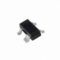
BFG590/X,215 NXP Semiconductors, BFG590/X,215 Datasheet - Page 2

BFG590/X,215
Manufacturer Part Number
BFG590/X,215
Description
TRANS NPN 15V 200MA SOT143B
Manufacturer
NXP Semiconductors
Datasheet
1.BFG590215.pdf
(11 pages)
Specifications of BFG590/X,215
Package / Case
SOT-143, SOT-143B, TO-253AA
Transistor Type
NPN
Voltage - Collector Emitter Breakdown (max)
15V
Frequency - Transition
5GHz
Power - Max
400mW
Dc Current Gain (hfe) (min) @ Ic, Vce
60 @ 70mA, 8V
Current - Collector (ic) (max)
200mA
Mounting Type
Surface Mount
Dc Collector/base Gain Hfe Min
60 @ 70 mA @ 8 V
Dc Current Gain Hfe Max
60 @ 70mA @ 8V
Minimum Operating Temperature
- 65 C
Mounting Style
SMD/SMT
Configuration
Single
Transistor Polarity
NPN
Maximum Operating Frequency
5000 MHz (Typ)
Collector- Emitter Voltage Vceo Max
15 V
Emitter- Base Voltage Vebo
3 V
Continuous Collector Current
0.2 A
Power Dissipation
400 mW
Maximum Operating Temperature
+ 175 C
Lead Free Status / RoHS Status
Lead free / RoHS Compliant
Gain
-
Noise Figure (db Typ @ F)
-
Lead Free Status / Rohs Status
Lead free / RoHS Compliant
Other names
934022990215
BFG590/X T/R
BFG590/X T/R
BFG590/X T/R
BFG590/X T/R
NXP Semiconductors
FEATURES
APPLICATIONS
DESCRIPTION
NPN silicon planar epitaxial transistor in a 4-pin
dual-emitter SOT143B plastic package.
MARKING
QUICK REFERENCE DATA
BFG590
BFG590/X
V
V
I
P
h
C
f
G
|S
TYPE NUMBER
SYMBOL
C
T
FE
High power gain
Low noise figure
High transition frequency
Gold metallization ensures excellent reliability.
MATV/CATV amplifiers and RF communications
subscriber equipment in the GHz range
Ideally suitable for use in class-A, (A)B and C amplifiers
with either pulsed or continuous drive.
CBO
CEO
tot
re
NPN 5 GHz wideband transistors
UM
21
|
2
collector-base voltage
collector-emitter voltage
collector current (DC)
total power dissipation
DC current gain
feedback capacitance
transition frequency
maximum unilateral power gain
insertion power gain
PARAMETER
CODE
%MH
%MN
open emitter
open base
T
I
I
I
I
f = 900 MHz; T
I
f = 900 MHz; T
Rev. 04 - 12 November 2007
C
C
C
C
C
s
= 35 mA; V
= 0; V
= 80 mA; V
= 80 mA; V
= 80 mA; V
60 C
CE
CONDITIONS
= 8 V; f = 1 MHz
CE
CE
CE
CE
PINNING
amb
amb
= 8 V
= 4 V; f = 1 GHz
= 4 V;
= 4 V;
= 25 C
= 25 C
PIN
1
2
3
4
handbook, 2 columns
Fig.1 Simplified outline SOT143B.
collector
base
emitter
emitter
Top view
1
4
BFG590
50
MIN.
BFG590; BFG590/X
DESCRIPTION
90
0.7
5
13
11
TYP.
MSB014
Product specification
3
2
collector
emitter
base
emitter
20
15
200
400
280
MAX.
BFG590/X
2 of 11
V
V
mA
mW
pF
GHz
dB
dB
UNIT


