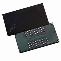
MT48LC16M16A2BG-75:D Micron Technology Inc, MT48LC16M16A2BG-75:D Datasheet - Page 22

MT48LC16M16A2BG-75:D
Manufacturer Part Number
MT48LC16M16A2BG-75:D
Description
DRAM Chip SDRAM 256M-Bit 16Mx16 3.3V 54-Pin VFBGA Tray
Manufacturer
Micron Technology Inc
Type
SDRAMr
Specifications of MT48LC16M16A2BG-75:D
Density
256 Mb
Maximum Clock Rate
133 MHz
Package
54VFBGA
Address Bus Width
15 Bit
Operating Supply Voltage
3.3 V
Maximum Random Access Time
6|5.4 ns
Operating Temperature
0 to 70 °C
Format - Memory
RAM
Memory Type
SDRAM
Memory Size
256M (16Mx16)
Speed
133MHz
Interface
Parallel
Voltage - Supply
3 V ~ 3.6 V
Package / Case
54-VFBGA
Organization
16Mx16
Address Bus
15b
Access Time (max)
6/5.4ns
Operating Supply Voltage (typ)
3.3V
Package Type
VFBGA
Operating Temp Range
0C to 70C
Operating Supply Voltage (max)
3.6V
Operating Supply Voltage (min)
3V
Supply Current
135mA
Pin Count
54
Mounting
Surface Mount
Operating Temperature Classification
Commercial
Lead Free Status / RoHS Status
Lead free / RoHS Compliant
Lead Free Status / RoHS Status
Compliant, Lead free / RoHS Compliant
Available stocks
Company
Part Number
Manufacturer
Quantity
Price
Company:
Part Number:
MT48LC16M16A2BG-75:D
Manufacturer:
Micron Technology Inc
Quantity:
10 000
Company:
Part Number:
MT48LC16M16A2BG-75:D TR
Manufacturer:
Micron Technology Inc
Quantity:
10 000
Electrical Specifications
Table 7: Absolute Maximum Ratings
Table 8: DC Electrical Characteristics and Operating Conditions
Notes 1–3 apply to all parameters and conditions; V
PDF: 09005aef8091e6d1
256Mb_sdr.pdf - Rev. N 1/10 EN
Voltage/Temperature
Voltage on V
Voltage on inputs, NC, or I/O balls relative to V
Storage temperature (plastic)
Power dissipation
Parameter/Condition
Supply voltage
Input high voltage: Logic 1; All inputs
Input low voltage: Logic 0; All inputs
Output high voltage: I
Output low voltage: I
Input leakage current:
Any input 0V ≤ V
Output leakage current: DQ are disabled; 0V ≤ V
Operating temperature:
DD
/V
IN
DDQ
≤ V
OUT
supply relative to V
Notes:
OUT
DD
Note:
= 4mA
(All other balls not under test = 0V)
= –4mA
Stresses greater than those listed may cause permanent damage to the device. This is a
stress rating only, and functional operation of the device at these or any other condi-
tions above those indicated in the operational sections of this specification is not
implied. Exposure to absolute maximum rating conditions for extended periods may
affect reliability.
1. V
1. All voltages referenced to V
2. The minimum specifications are used only to indicate cycle time at which proper opera-
3. An initial pause of 100μs is required after power-up, followed by two AUTO REFRESH
4. V
V
tion over the full temperature range is ensured; (0°C ≤ TA ≤ +70°C (commercial), –40°C ≤
TA ≤ +85°C (industrial), and –40°C ≤ TA ≤ +105°C (automotive)).
commands, before proper device operation is ensured. (V
up simultaneously. V
mand wake-ups should be repeated any time the
be greater than one-third of the cycle rate. V
width ≤3ns.
DD
DD
IH
overshoot: V
.
and V
SS
DDQ
SS
must be within 300mV of each other at all times. V
OUT
Commercial
Industrial
Automotive
IH,max
DD
≤ V
/V
SS
DDQ
DDQ
= V
and V
DDQ
= +3.3V ±0.3V
22
SS
SSQ
.
+ 2V for a pulse width ≤ 3ns, and the pulse width cannot
V
Symbol
must be at same potential.) The two AUTO REFRESH com-
DD
V
V
V
V
I
, V
T
T
T
OZ
I
OH
OL
IH
L
IL
A
A
A
Micron Technology, Inc. reserves the right to change products or specifications without notice.
DDQ
IL
V
Symbol
Min
undershoot: V
DD
–0.3
–40
–40
2.4
–5
–5
T
3
2
–
0
V
256Mb: x4, x8, x16 SDRAM
/V
STG
–
t
IN
REF refresh requirement is exceeded.
DDQ
Electrical Specifications
DD
Min
–55
–1
–1
V
–
and V
© 1999 Micron Technology, Inc. All rights reserved.
DD
IL,min
Max
+105
+0.8
+70
+85
3.6
0.4
–5
5
–
+ 0.3
Max
+150
DDQ
+4.6
+4.6
DDQ
= –2V for a pulse
1
must not exceed
must be powered
Unit
Unit
°C
W
μA
μA
V
˚C
˚C
˚C
V
V
V
V
V
Notes
Notes
1
4
4


