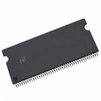
MT48LC2M32B2P-7:G TR Micron Technology Inc, MT48LC2M32B2P-7:G TR Datasheet - Page 63

MT48LC2M32B2P-7:G TR
Manufacturer Part Number
MT48LC2M32B2P-7:G TR
Description
DRAM Chip SDRAM 64M-Bit 2Mx32 3.3V 86-Pin TSOP-II T/R
Manufacturer
Micron Technology Inc
Type
SDRAMr
Datasheet
1.MT48LC2M32B2P-6G_TR.pdf
(69 pages)
Specifications of MT48LC2M32B2P-7:G TR
Density
64 Mb
Maximum Clock Rate
143 MHz
Package
86TSOP-II
Address Bus Width
13 Bit
Operating Supply Voltage
3.3 V
Maximum Random Access Time
17|8|5.5 ns
Operating Temperature
0 to 70 °C
Format - Memory
RAM
Memory Type
SDRAM
Memory Size
64M (2Mx32)
Speed
143MHz
Interface
Parallel
Voltage - Supply
3 V ~ 3.6 V
Package / Case
86-TSOP
Organization
2Mx32
Address Bus
13b
Access Time (max)
17/8/5.5ns
Operating Supply Voltage (typ)
3.3V
Package Type
TSOP-II
Operating Temp Range
0C to 70C
Operating Supply Voltage (max)
3.6V
Operating Supply Voltage (min)
3V
Supply Current
160mA
Pin Count
86
Mounting
Surface Mount
Operating Temperature Classification
Commercial
Lead Free Status / RoHS Status
Lead free / RoHS Compliant
Other names
557-1073-2
Figure 45:
PDF: 09005aef811ce1fe/Source: 09005aef811ce1d5
64MSDRAMx32_2.fm - Rev. J 12/08 EN
COMMAND
BA0, BA1
DQM 0-3
A0-A9
CKE
CLK
A10
DQ
t CKS
t CMS
t AS
t AS
t AS
WRITE – Without Auto Precharge
ACTIVE
T0
ROW
ROW
BANK
t CKH
t CMH
t AH
t AH
t AH
Notes:
t RCD
t RAS
t RC
t CK
T1
NOP
1. For this example, BL = 4, and the WRITE burst is followed by a “manual” PRECHARGE.
2. Faster frequencies require two clocks (when
3. A8 and A9 = “Don’t Care.”
4.
t
WR of 1 CLK available if running 100 MHz or slower. Check factory for availability.
DISABLE AUTO PRECHARGE
t CMS
t CL
t DS
COLUMN m 3
WRITE
BANK
T2
D
IN
t CMH
t CH
t DH
m
t DS
D
IN
T3
NOP
m + 1
t DH
t DS
63
D
IN
T4
NOP
m + 2
t DH
Micron Technology, Inc., reserves the right to change products or specifications without notice.
t DS
D
NOP
IN
T5
m + 3
t DH
t
WR >
t WR
SINGLE BANK
PRECHARGE
t
ALL BANKs
2
CK).
BANK
T6
©2001 Micron Technology, Inc. All rights reserved.
NOP
t RP
T7
64Mb: x32 SDRAM
Timing Diagrams
ACTIVE
ROW
ROW
BANK
T8
DON’T CARE
UNDEFINED


