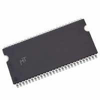
MT48LC4M16A2TG-75 IT:G TR Micron Technology Inc, MT48LC4M16A2TG-75 IT:G TR Datasheet - Page 43

MT48LC4M16A2TG-75 IT:G TR
Manufacturer Part Number
MT48LC4M16A2TG-75 IT:G TR
Description
DRAM Chip SDRAM 64M-Bit 4Mx16 3.3V 54-Pin TSOP-II T/R
Manufacturer
Micron Technology Inc
Type
SDRAMr
Datasheet
1.MT48LC4M16A2P-75G_TR.pdf
(72 pages)
Specifications of MT48LC4M16A2TG-75 IT:G TR
Package
54TSOP-II
Density
64 Mb
Address Bus Width
14 Bit
Operating Supply Voltage
3.3 V
Maximum Clock Rate
133 MHz
Maximum Random Access Time
6|5.4 ns
Operating Temperature
-40 to 85 °C
Format - Memory
RAM
Memory Type
SDRAM
Memory Size
64M (4M x 16)
Speed
133MHz
Interface
Parallel
Voltage - Supply
3 V ~ 3.6 V
Package / Case
54-TSOP II
Lead Free Status / RoHS Status
Contains lead / RoHS non-compliant
Other names
557-1090-2
PDF: 09005aef80725c0b/Source: 09005aef806fc13c
64MSDRAM_2.fm - Rev. N 12/08 EN
10. For a READ without auto precharge interrupted by a READ (with or without auto pre-
11. For a READ without auto precharge interrupted by a WRITE (with or without auto pre-
12. For a WRITE without auto precharge interrupted by a READ (with or without auto pre-
13. For a WRITE without auto precharge interrupted by a WRITE (with or without auto pre-
14. For a READ with auto precharge interrupted by a READ (with or without auto precharge),
15. For a READ with auto precharge interrupted by a WRITE (with or without auto precharge),
16. For a WRITE with auto precharge interrupted by a READ (with or without auto precharge),
17. For a WRITE with auto precharge interrupted by a WRITE (with or without auto precharge),
6. All states and sequences not shown are illegal or reserved.
7. READs or WRITEs to bank m listed in the Command (Action) column include READs or
8. Concurrent Auto precharge: Bank n will initiate the auto precharge command when its
9. Burst in bank n continues as initiated.
WRITEs with auto precharge enabled and READs or WRITEs with auto precharge disabled.
burst has been interrupted by bank m’s burst.
charge), the READ to bank m will interrupt the READ on bank n, CL later (Figure 12 on
page 25).
charge), the WRITE to bank m will interrupt the READ on bank n when registered
(Figures 14 and 15 on page 27). DQM should be used one clock prior to the WRITE com-
mand to prevent bus contention.
charge), the READ to bank m will interrupt the WRITE on bank n when registered (Figure 22
on page 32), with the data-out appearing CL later. The last valid WRITE to bank n will be
data-in registered one clock prior to the READ to bank m.
charge), the WRITE to bank m will interrupt the WRITE on bank n when registered
(Figure 20 on page 31). The last valid WRITE to bank n will be data-in registered one clock
prior to the READ to bank m.
the READ to bank m will interrupt the READ on bank n, CL later. The precharge to bank n
will begin when the READ to bank m is registered (Figure 29 on page 37).
the WRITE to bank m will interrupt the READ on bank n when registered. DQM should be
used two clocks prior to the WRITE command to prevent bus contention. The precharge to
bank n will begin when the WRITE to bank m is registered (Figure 30 on page 38).
the READ to bank m will interrupt the WRITE on bank n when registered, with the data-out
appearing CL later. The precharge to bank n will begin after
when the READ to bank m is registered. The last valid WRITE to bank n will be data-in regis-
tered one clock prior to the READ to bank m (Figure 31 on page 38).
the WRITE to bank m will interrupt the WRITE on bank n when registered. The precharge to
bank n will begin after
tered. The last valid WRITE to bank n will be data registered one clock prior to the WRITE to
bank m (Figure 32 on page 39).
t
WR is met, where
43
Micron Technology, Inc., reserves the right to change products or specifications without notice.
t
WR begins when the WRITE to bank m is regis-
64Mb: x4, x8, x16 SDRAM
t
WR is met, where
©2000 Micron Technology, Inc. All rights reserved.
Commands
t
WR begins


